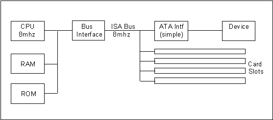
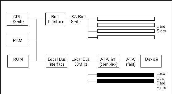
- C.2 Termination
When analyzing the ATA bus, the standard 18-inch ribbon cable used to connect devices could be considered to be either a transmission line or a lumped LC circuit. Analog circuit designers generally use the rule of thumb that if the edge rate is less than four times the cable propagation delay, then it is a transmission line. Otherwise it can be considered to be a lumped LC.
Note C.2 - Different ratios are used by different designers. A survey of textbooks shows that values of three times, four times, six times, and even sqrt(2*pi) have been suggested.
The cable used almost exclusively is a PVC-coated 40-conductor ribbon cable with 0,05 inch spacing. This cable can be modeled as a transmission line with a typical characteristic impedance of 110 ohms and propagation velocity of 60% c. This gives a propagation delay of 2,5 ns. The edge rates from both hosts and devices are usually faster than 10 ns (4 x 2,5 ns), so a transmission line model applies.
Note C.3 - Measurements taken on a sample cable gave an impedance of 107 ohms and a delay of 2,6 ns (59% c propagation velocity).
- C.2.1 The problem
Many users have experienced problems with early implementations of PIO Mode 3 devices and hosts. Most failures in the systems observed can be attributed to signal integrity problems on the control lines that go from the host to the device. The problem appears most frequently as ringing on the DIOR- (read command) and DIOW- (write command) lines.
During a read cycle when DIOR- is asserted, it is possible for the ringing to create a short duration deassertion pulse (see figure C.3). This pulse occurs early in the read cycle. Inside the ATA interface portion of the datapath controller chip is a FIFO buffer that contains the data to be read. The extra pulse on the DIOR- line advances the FIFO pointer by one. This results in losing one word of data. The host system read operation therefore receives one word too few, and the remaining bytes are shifted. A typical data sequence might look like . . .W7, W8, W9, W11, W12 . . . Notice that word 10 is missing from the returned data. This also means that the host tries to read one more word from the device than the device has remaining. Depending on the implementation of the BIOS, this locks-up the system or simply returns a byte of garbage at the end of the sector.
Pulse slivers due to ringing on the DIOW- line cause a similar problem during writes. The pulse sliver advances the FIFO pointer by one unexpectedly, writing an extra word of garbage into the FIFO. Subsequent data bytes are shifted by one word. A typical stored data sequence on the device might look like . . . W7, W8, W9, XX, W10, W11 . . . In this example an extra word was inserted during the write cycle for word 10. From the device's point of view, the host is trying to write 514 bytes rather than the expected 512 bytes. The device throws away the final word and should flag an error. A properly written BIOS detects this error and indicates a problem to the user.
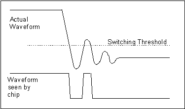
Figure C.3 – Typical ringing on ATA bus and its effect
These are only two examples of a systemic problem. Ringing on any control signal, and possibly on data lines, can cause system failures or data loss. To address this problem it is necessary to examine the circuit structure of the ATA bus.
Figure C.4 shows the seven basic driver/receiver structures that appear in ATA bus interfaces. The host circuitry appears on the left side of the diagram and the device circuitry appears on the right. The first circuit in figure C.4 shows the structure of the seven control lines that go from the host to the device. A SPICE model of the circuit is designed if some assumptions are made about the circuitry at the host and device. Virtually all devices today use a CMOS VLSI chip as part of the bus interface. This high-impedance input is modeled with clamp diodes to supply and ground and a typical input capacitance of 8 pF (see figure C.4). Since the ringing problem is worse with CMOS VLSI bridge chips at the source the host is modeled as a voltage source with 1 ns edges, a 12 ohm output impedance, and clamp diodes to supply and ground. The ribbon cable is modeled as a 110 ohm transmission line. The resulting SPICE model appears in figure C.5.
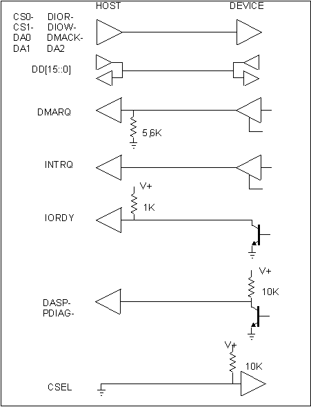
Figure C.4 – The seven basic ATA driver/receiver structures
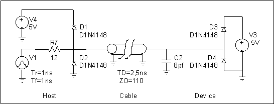
Figure C.5 – Schematic of SPICE simulation model
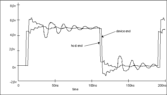
Figure C.6 – Simulation waveforms at host and device ends of cable
The simulation results in figure C.6 show the waveforms at both the host and device ends of the cable. The signal at the device end has ringing of sufficient amplitude to cause false triggering of the device. This is confirmed by transmission line theory which indicates that ringing will occur whenever the source impedance is lower than the characteristic impedance of the cable, and the termination is of higher impedance than the cable. The greater the mismatch, the greater the amplitude of the ringing. The oscilloscope trace shown in figure C.7 confirms the results of the simulations.
The latest trend in ATA interface chips has aggravated the ringing problem. In an effort to decrease propagation delay, some bridge chip manufacturers have increased the output drive current of the host in order to slew the output signal faster with the capacitive load of the cable. This has caused the edge rates and the output impedance to decrease, both of which increase the ringing at the device end of the cable. The oscilloscope trace in figure C.7 uses a generic driver and receiver – the problem of ringing is a fundamental characteristic of the ATA interface. This has not always been the case.
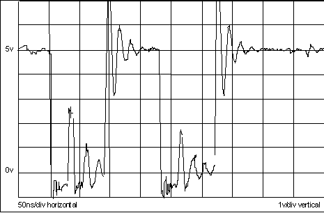
Figure C.7 – Oscilloscope trace at device end of DIOR- signal
on a typical system
- C.2.2 What are the options?
The proper solution is to terminate the transmission line. Either a series termination at the source or a parallel termination at the device is acceptable. Unfortunately, each of these solutions has problems of its own. A 110 ohm termination at the device end causes excessive DC loading. Having a termination on both devices in a master/slave two device configuration results in too low of a load impedance, causing reflections on the cable again.
Matching the source impedance of the host to the cable has similar problems. The impedance required is different when the host is in the middle of the cable as opposed to being at the end. Even with the host at one end of the cable, ringing can occur with a two device configuration. This is because the input impedance of the devices is not infinite: they appear as a reactive load due to their input stray capacitance.
The SCSI interface standard avoids ringing by requiring terminations at each end of the physical cable and having each device drive the cable with a current sink. However, real SCSI configurations often have too many, too few, or improperly located terminations. Changing the ATA standard to a user-installed termination scheme loses all backward compatibility and therefore is not considered to be a viable option.
One of the solutions used in the past to "fix" failing ATA configurations has been to place a capacitor at the input of the device. Since the ringing is the result of a resonant system, adding purely reactive elements (capacitors and inductors) which simply change the frequency of oscillation is not recommended. These elements may fix a given configuration of a device and cable, but they really just move the interfering resonance peaks to a different frequency, solving the problem only for that particular configuration. Proper solutions include resistive elements to dissipate the energy stored in the transmission line.
No single solution meets the dual criteria of solving the ringing problem and being backward compatible with current systems. The suggested approach uses partial solutions in three different areas: partial termination at the host, partial termination at the device, and edge rate control at both the host and the device.
- C.2.3 Design goals
Before a solution can be designed the design goals must be explicitly stated. This leads to the question of "How much ringing is acceptable?" To answer this question the design and specification of the ATA bus is considered.
The ATA bus was originally designed to use standard TTL signals. TTL was designed with built-in noise margin. All drivers are required to have a "low" (zero) signal level of 0,5 V or less, and a "high" (one) signal level of 2,4 V or more. All receivers are specified to accept any signal below 0,8 V as a logical zero and any signal above 2,0 V as a logical one. This results in a low-side noise margin of 0,3 V (0,8 - 0,5) and a high-side margin of 0,4 V (2,4 - 2,0). Signals between 0,5 V and 2,0 V are in no man’s land, interpreted by the receiver as either a zero or a one. TTL compatible inputs typically use a switching threshold of 1,3 to 1,4 V.
Bus designers have long known that the noise margins of TTL are insufficient for signals passed on cables. To improve the noise margin inherent in TTL systems hysteresis has been added to the receiver input. Hysteresis changes the input switching threshold depending on the present state of the logic output of the receiver. For example, if the receiver is currently in a zero state, it might require an input voltage of 1,7 V before changing to a one. Once in a one state, the receiver might require the input voltage to drop below 0,9 V before changing back to a zero. Modern design practice dictates that all signals passing across a bus be received with hysteresis.
It is desirable that, even with ringing, the input signal remain less than 0,5 V after a falling edge and remain above 2,4 V after a rising edge. With CMOS drivers only the falling edge is of concern. This is due to the input switching threshold of TTL (typically 1,4 V) being closer to ground than to the supply. It turns out that designing to the 0,5 V requirement is too restrictive, so the looser requirement of 0,8 V is used here. This relaxed requirement essentially removes the noise margin inherent in TTL and depends on receiver hysteresis for proper operation. As input hysteresis has been the norm in drive design for many years now, this limitation is not considered unreasonable.
Depending on system timing and other issues, a designer may elect to use a looser threshold of 0,9 V or a tighter one of 0,7 V. For these cases circuit simulation of the bus and receiver is done to verify the design. The resulting termination circuits have different values from those derived here.
- C.2.4 Source termination
A series resistor at the source (host) acts as a termination to the transmission line. When the value of the resistor matches the characteristic impedance of the cable (110 ohms) then the ringing is reduced to zero. Resistor values less than 110 ohms will partially terminate the cable and reduce the ringing.
Note C.3 - This assumes that the output impedance of the driver is zero. In reality, optimum match occurs when the output impedance and the series resistor together equal the cable impedance.
The ATA specification requires that a source sink 4 mA while maintaining a logical low output voltage of 0,5 V or less (See 4.3). Adding a series resistor in the output of the driver causes the output logical zero voltage to increase with greater resistance. For example, if the unterminated logical zero output of the driver is 0,4 V, then a maximum series resistance of 25 ohms is allowed ( (0,5-0.4)/4mA ). This DC voltage drop requirement acts in opposition to the higher resistance values required for cable termination. A five-percent, 22 ohm resistor meets the 25 ohm requirement. Note that this places an addition requirement on the host interface chip: timing measurements use a logical threshold of 0,4 V rather than 0,5 V as in the past.
Is a 22 ohm resistor adequate for reducing the ringing? The simulation was repeated using the same model as shown in figure C.5 with a 22 ohm series resistor added. The results of that simulation appear in figure C.8. The ringing is significantly reduced from the previous simulation in figure C.6.
For maximum ringing it is assumed that the device(s) have CMOS input stages that do not provide significant DC loading. Yet for the series termination resistor calculation it is assumed a logical low sink current of 4 mA. Both of these conditions cannot simultaneously occur in practice, but assuming the worst-case sink current gives the best compatibility with older devices.
Figure C.8 – Waveforms with 22 ohm series resistor at source
- C.2.5 Receiver termination
Receiver termination is more difficult than source termination. Viable solutions must work with one or two drives located anywhere along the cable. The host may be located at one end or in the middle of the cable. The host may or may not have termination. These and other considerations make drive termination a multifaceted problem.
The first constraint is the maximum DC loading allowed. The ATA specification requires that the host be capable of providing 400 µA of current while in a logical one state. Assuming each device is allowed to take half of that amount, the minimum DC resistance allowed is 25K ohms.
Note C.4 - This assumes a CMOS output with a high output voltage of 5,0 V : 5,0V/200µA = 25KW
For a 110 ohm transmission line, 25K ohms is as good as infinity. This means that any practical termination solution must not have significant DC loading.
One way of terminating the cable is with an "AC termination." This is a simple RC network that provides termination for high-frequency signals but does not load the line at DC (see figure C.9). This circuit acts as both a cable termination and a filter for the ringing. The termination characteristics can be observed by looking at the ringing signal at the host when the circuit is connected or removed. When the circuit is in place, less energy is reflected back to the host, so the host waveform has less ringing. The lowpass filter characteristics of the circuit help decrease the amount of ringing presented to the interface circuitry of the device.
Although this may appear to be an unusual method of terminating the cable, it is not without precedent. The IEEE P996 committee recognized the problems inherent in the design of the IBM PC/ATÔ
bus and recommended a series RC termination for increased "data integrity and system reliability." They suggested that the termination circuit be added to each end of the backplane or motherboard. The recommended values are 40 to 60 ohms for the resistor and 30 to 70 pF for the capacitor.
Deriving the optimum values for an ATA bus AC termination circuit is difficult. The easiest way of determining the values is to perform a number of trial-and-error SPICE simulations for different host and device configurations. The recommended values are 82 ohms and 10 pF. Simulations show that capacitance values between 8 pF and 20 pF work well. Since the input capacitance of many interface chips is between 8 and 10 pF, a discrete capacitor is often unnecessary. This reduces the cost of implementation on the device. A conservative approach is to place pads so additional capacitance can be added if required.
Device manufacturers need to insure that any partial termination circuits they implement present an effective capacitance of 20 pF or less. What is an effective capacitance? From a practical point of view, any circuit is valid provided it does not increase the propagation delay of a worst-case cable. This is because systems manufacturers are counting on a certain cable delay in their design. The easiest way to answer the question of acceptability is to run a SPICE simulation and measure the delay. The simulation should be run twice: once with a simple 20 pF load, and again with the proposed termination circuit. If the resulting delay of the proposed termination circuit is less than or equal to that obtained with a 20 pF load, then it meets the criterion for acceptance. The recommended termination of 82 ohms and 10 pF passes the test.
The major drawback of the RC termination circuit is that it adds delay to the signal. Since the ATA specification defines the timing at the input to the device (see clause 10), device manufacturers must insure that their interface chip still works properly with the additional delay. The delay can be calculated for rising edges (2,0 V threshold) and falling edges (0,8 V threshold) with a fairly straightforward SPICE simulation. For the 82 ohm and 10 pF termination the delay is less than 1,5 ns.
Note C.5 - 0,7 ns for the rising edge, 1,2 ns for the falling edge, derived from simulations.
Will termination at both the host and the device "over-terminate" the transmission line? Figure C.10 shows the simulation results for device termination with no host termination, and figure C.11 shows the same simulation with a 22 ohm host termination added. It is clear that termination at both the host and the device results in the best signal integrity. To completely confirm the validity of the termination circuits more simulations must be performed with source termination and two devices with receiver termination; two devices, one with and one without termination; etc.
Another option for controlling ringing at the device is the use of a clamping circuit. Biased diodes have been shown to be excellent solutions, reducing the ringing to virtually zero. The advantage of clamp circuits is that they do not require any components in series with the signal, and therefore do not add any delay. This is particularly important for PIO Mode 4 operation. The disadvantage of clamping circuits is that they take considerably more space on the circuit board and cost much more than passive elements. Some implementations have used clamping circuits on sensitive edge-triggered lines (such as DIOR- and DIOW-) and used passive terminations on less sensitive lines (such as data). Clamping circuits work well both with and without host-end termination and are worthy of further investigation.
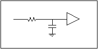
Figure C.9 – AC termination circuit at device end of cable
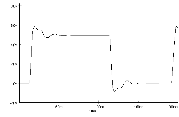
Figure C.10 – Device waveform with device termination and no host termination
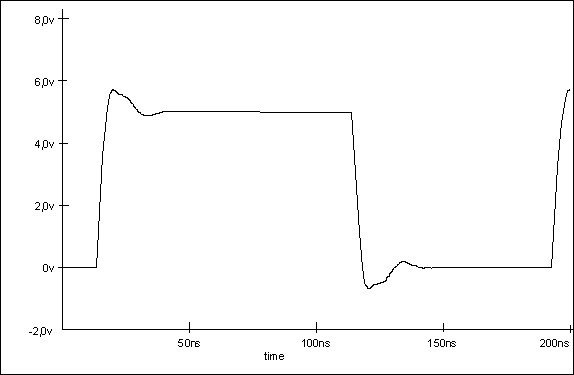
Figure C.11 – Device waveform with both device and host terminations
- C.2.6 Edge rate control
The ATA specification requires that all sources have a rise time of not less than 5 ns (See 4.3). The original intent of this requirement was to avoid transmission line problems on the bus. One of the common misconceptions is that limiting the rise time of the source to 5 ns will fix the ringing problem.
A rule-of-thumb for analog designers is that when the propagation delay of the cable exceeds one-quarter of the signal rise time, cable termination be used.
Note C.6 - In reality this rule-of-thumb varies considerably. Various books use values of one-half, one-third, one-fifth, and even one over the square root of two times pi.
In the case of the ATA bus, the worst case propagation delay of the cable is approximately 4 ns so by this rule rise times of less than 16 ns require termination. Many local bus to ATA bridge chips available today have rise times of 1 to 2 ns, in violation of the ATA requirement of 5 ns.
Note C.7 - Assuming 18-inch cable, 60% c velocity factor; two drives, each drive having a maximum load of 25 pF.
The ATA document says that the rise time must be a minimum of 5 ns into a 40 pF load. The easiest way to implement this from a chip designer’s point of view is to decrease the drive of the I/O cell until the timing requirement is met. Unfortunately, very few systems in the real world ever approach 40 pF. Although the cable and the devices have maximum capacitance specifications, these capacitance values are never seen by the host. At DC and low frequencies the cable looks like a capacitor. But at high frequencies (or fast edge rates) the cable appears as a transmission line.
One of the results from transmission line theory is that a properly terminated transmission line appears to be a resistor with no capacitance or inductance. From the driving end of the line the transmission line looks just like a resistor whose value is the characteristic impedance of the line. The distributed capacitance of the transmission line does not appear as a capacitive load: it interacts with the inductance of the line and the termination to appear resistive. As a result, real-world systems rarely see more than 30 pF of capacitive loading at the host. The reduced capacitance causes the I/O cell to slew faster, creating rise times less than 5 ns.
The best solution is to use special I/O cells that have slew rate feedback to keep the rise time at 5 ns regardless of load. These are more difficult to design than conventional I/O cells and consume more die area. This could be a problem for interface chip designs that are already pad ring limited. Another approach is to use a conventional I/O cell that is designed to have 5 ns rise times into a 10 pF or 20 pF load. The total delay of the cell is greater for heavier loads, but the maximum delay is determined with SPICE modeling of a worst-case cable and load.
Rise time control is still an important tool for controlling ringing. Although it is not the total solution, simulations show marked improvement between sources with 1 ns rise times and sources with 5 ns rise times. Slower rise times give the added benefit of reduced crosstalk.
- C.2.7 The solution: A combination
No one element – source termination, receiver termination, nor rise time control – completely addresses the problem of ringing on the ATA bus. The recommended solution is a combination of all three. Each item must be enough to exert some control over the ringing problem in order to maintain backward compatibility. With the faster transfer rates of PIO Mode 4 (and DMA Mode 2) it is even more important to control undesired ringing on the bus.
The above discussion only addressed a particular group of signals driven by the host and received by the device. There are other signals driven by the device and received by the host that are equally susceptible to ringing. These signals need termination, but in the opposite manner. The device inserts 22 ohm resistors in series with signals it drives and the host has an RC (or just R) receiving end termination.
The data lines are different in that they are data bidirectional. Strictly speaking, the data lines are not edge sensitive and are unaffected by ringing. This is true as long as the data signals have sufficient setup time to allow for bus settling. The settling time is as long as 60 ns in severe cases. Excessive ringing on the data lines induces spurious signals on adjacent control lines (crosstalk). Good design dictates that some type of ringing control be used on data lines, but perhaps not as much as on edge-sensitive control lines. A good compromise is to insert 22 ohm series resistors on data lines at both the host and the device. The driving end sees the same source termination as before. The receiving end sees an RC network of 22 ohms combined with the input capacitance of the interface chip. This is enough to substantially reduce the ringing and minimize settling time.
The one remaining bus structure not discussed is the open collector output driven by the device (IORDY). This signal is driven by a current source rather than a voltage source. Usually the transistor driving this signal is relatively slow and does not cause an excessive amount of ringing. The nature of IORDY makes it relatively insensitive to ringing that might occur.
Table C.1 summarizes the recommended changes to the signal lines on the ATA bus:
Table C.1 - Recommended termination
|
Signal Name |
Host Termination |
Device Termination |
|
DIOR-, DIOW- |
22 ohm series |
82 ohm series |
|
CS0-, CS1- |
22 ohm series |
82 ohm series |
|
DA0, DA1, DA2 |
22 ohm series |
82 ohm series |
|
DMACK- |
22 ohm series |
82 ohm series |
|
RESET- |
no change |
no change |
|
DD0 through DD15 |
22 ohm series |
22 ohm series |
|
DMARQ |
82 ohm series |
22 ohm series |
|
INTRQ |
82 ohm series |
22 ohm series |
|
IORDY |
no change |
no change |
|
DASP-, PDIAG- |
no change |
no change |
|
CSEL |
no change |
no change |
|
Note: For the 82 ohm series termination, an additional parallel capacitor may be needed if the interface chip and circuit board layout have less than 8 pF of capacitance. |
- C.2.7.1 Example of device-end termination timing
Assume that 82 ohm series resistors are inserted on all receive signals and 22 ohm series resistors on all transmit and bidirectional signals. Also assume that the input capacitance of the interface chip is 10 pF. There are three different RC configurations that occur (see figure C.12). All receive signals will see an 82 ohm and 10 pF network. The data lines will see a 22 ohm and 10 pF network when the device is receiving data. Signals driven back to the host (including data lines during a read) will see 22 ohms and 50 pF. The 50 pF assumption is the worst-case condition of both the host and another device being located nearby (negligible cable length), and both of them having the maximum allowed input capacitance.
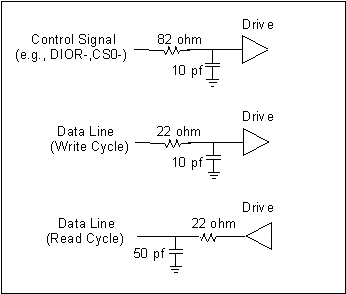
Figure C.12 – Signal models for device-end timing calculations
A simple SPICE simulation with a signal source and an RC load will show what the delays are through these three networks. Because the switching thresholds are not symmetrical with respect to the supply (0,8 V and 2,0 V) the delay for rising edges is different than that for falling edges. Since the input edge rate is unknown, both fast and slow edge inputs are simulated. The worst-case delay occurs with slow edges for rise times and fast edges for fall times. This mixture of slow rise time and fast fall time does not occur in real life, but since the edge speed is not known the worst case is planned for. The SPICE signal source is programmed for a rise time of 6,25 ns (same as 5 ns for 10% to 90%) and a fall time of 0,1 ns. The net result is six delay values. The results of the SPICE simulations are shown in table C.2.
Table C.2 – Typical device-end propagation delay times
|
Symbol |
Description |
Value |
|
Tphlc |
Propagation delay, high to low, control line |
1,0 ns |
|
Tplhc |
Propagation delay, low to high, control line |
0,9 ns |
|
Tphldi |
Propagation delay, high to low, data in |
0,5 ns |
|
Tplhdi |
Propagation delay, low to high, data in |
0,3 ns |
|
Tphldo |
Propagation delay, high to low, data out |
2,5 ns |
|
Tplhdo |
Propagation delay, low to high, data out |
1,1 ns |
These delay values, combined with the interface chip timing specifications, will give the timing at the pins of the device. The trick is to figure out how each one of the ATA timing parameters is affected by the delays.
For example, consider the DIOW- Data Setup time (ATA value t3). This is the amount of time that the data must be stable before the rising edge of DIOW-. Assume that the interface chip has a value of 2,0 ns. It is known that DIOW- is a control signal and the rising edge of control signals are delayed by 0,9 ns. This means that the setup time at the chip is actually greater than expected. But the data is delayed too. It is not known what the data pattern is so it is assumed that the delay time is the maximum of Tphldi and Tplhdi. The actual setup time is 2,0 + 0,9 - MAX(0,3, 0,5) = 2,4 ns. This is less than the ATA requirement of 30 ns (for PIO Mode 3) and therefore within spec.
This careful thought process must be repeated for all fifteen of the ATA PIO timing parameters (and for DMA also). The easiest way to do this is to make a spreadsheet and enter the six values for RC delay and the interface chip timing parameters. Spreadsheet formulas can then compute the timing at the pins of the device and highlight any that are not within spec. In this manner the difficult calculations need only be derived once and it becomes easier to verify results.
- C.2.7.2 Example of host-end termination timing calculation
The host-end timing calculations are similar to the device-end calculations described above with a few more complicating factors added in. The four different signal configurations are shown in figure C.13. For this design 82 ohm series resistors are used on control lines received by the host and 22 ohm resistors on the data lines and control lines driven by the host. It is assumed that the host adapter chip input capacitance plus stray capacitance is 15 pF.
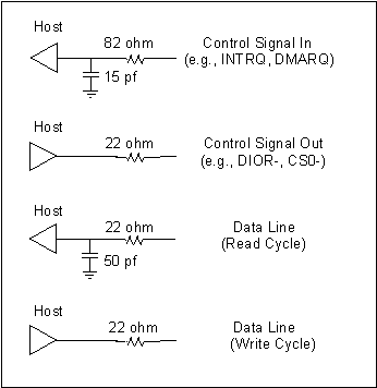
Figure C.13 – Host-end signal configurations with terminations
For these values, the control signal out and the data out models look the same. One simulation can be used to determine both values. The greatest uncertainty is the delay through the cable for received signals. The total cable delay depends on the source impedance of the device. This can be anything from zero to 82 ohms; the greater the impedance, the greater the delay. It is assumed for this example that the device vendor has read this document and has decided to use 22 ohms resistors. If it is desired later to make a worst-case assumption of 82 ohms, then approximately 2 ns are added to the numbers.
Using SPICE models similar to the one shown in figure C.14 the eight delay parameters required are derived. A second device appears in the model as a lumped capacitance of 25 pF which causes the maximum delay. The resulting values appear in table C.3. By examining the values in the table it should be clear why the cable propagation delay is often referred to as being about 5 ns.
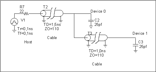
Figure C.14 – SPICE model for control signal out delay calculation
Table C.3 – Typical host-end propagation delay times
|
Symbol |
Description |
Value |
|
Tphlci |
Propagation delay, high to low, control in |
6,4 ns |
|
Tplhci |
Propagation delay, low to high, control in |
4,7 ns |
|
Tphlco |
Propagation delay, high to low, control out |
5,9 ns |
|
Tplhco |
Propagation delay, low to high, control out |
4,6 ns |
|
Tphldi |
Propagation delay, high to low, data in |
5,7 ns |
|
Tplhdi |
Propagation delay, low to high, data in |
4,3 ns |
|
Tphldo |
Propagation delay, high to low, data out |
5,9 ns |
|
Tplhdo |
Propagation delay, low to high, data out |
4,6 ns |
The process of finding the ATA timing values is the same as for the device-end example. The propagation delay times are added to and subtracted from the host adapter chip timings to obtain the timings at the input to the device, in this case calculating the timing at the drive furthest from the host adapter. The resulting timing values are compared against the ATA values to determine what mode the device operates at.
- C.2.8 Dual port cabling
One of the recent enhancements to the ATA bus has been the use of primary and secondary ports, allowing the user to attach up to four devices. The optimal way to implement dual ports is to have two completely separate interfaces that have no circuitry in common. This guarantees isolation between the ports and insures that no interference will occur.
Note C.8 - At the 1995 Windows Hardware Engineering Conference (WinHEC), Microsoft recommended the use of fully independent primary and secondary ports.
The advent of local bus bridge chips has introduced new driving forces to the dual port cabling issue. Implementing two independent ATA ports on a single chip requires 66 I/O pins. Due to the cost of pins, some designs have combined the data lines of the two ports into one set of pins. Sharing the data lines (or any other lines) in this way without termination is asking for trouble. Simulations confirm that the ringing in such configurations is large and complex, particularly if the loads on the two cables are not balanced.
One alternative pin-saving solution would be to add a set of external buffers. This would require three new control lines but would save sixteen data lines for a net improvement of thirteen pins. This also would require additional packages on the circuit board.
An economical solution is to add independent series resistors for each line (see figure C.15). Energy reflected back from the first cable passes through one termination resistor before getting to the host. The reflected signal is further attenuated as it passes through the second resistor and into the second cable. This signal is reflected from the end of the second cable (with loss), and must pass through the termination resistor again before arriving at the host. This provides sufficient attenuation of reflected signals.
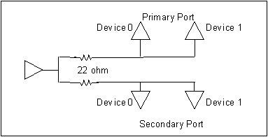
Figure C.15 – Preferred connection for shared lines in dual port systems
Not all of the signal lines in a shared dual port interface can be shared. If the chip selects (CS0-, CS1-) and the data strobes (DIOR-, DIOW-) are shared, then it is impossible to differentiate between the primary and secondary ports. A write to a device on one port causes the same action to occur on the other port, destroying the data on the other device. The data strobe lines are sensitive edge-triggered signals while the chip selects act more like level-sensitive address lines. It is recommended that designers share the less sensitive chip selects and not share the data strobes.
Table C.4 makes some assumptions about how the dual porting is being implemented. If the data lines are shared, there are not simultaneous accesses to the primary and secondary ports. This in theory allows the DMACK- and IORDY lines also to be shared. The INTRQ and DMARQ signals are driven by tristate buffers on the devices. Either the master or slave enables its tristate driver depending on the state of the DEV bit in the Device/Head Register. Therefore INTRQ and DMARQ cannot be shared because either the master or slave device will be driving these lines at all times. The primary port devices do not know about the secondary port devices, so sharing these lines would create a conflict. In theory the DMACK- line could be shared since it is driven by the host. In practice this is not recommended. It is likely that some devices respond unconditionally to the DMACK- signal, whether they ever requested a DMA cycle or not. This could lead to a conflict on a DMA cycle between a primary port device and a secondary port device during the data cycle. For these reasons the INTRQ, DMARQ, and DMACK- lines cannot be shared.
Table C.4 – Possible sharing of ATA signals in dual port configurations
|
Signal name |
|
|
DIOR-, DIOW- |
Not shareable |
|
CS0-, CS1- |
Shareable |
|
DA0, DA1, DA2 |
Shareable |
|
DMACK- |
Not shareable |
|
RESET- |
Shareable |
|
DD0 – DD15 |
Shareable |
|
DMARQ |
Not shareable |
|
INTRQ |
Not shareable |
|
IORDY |
Shareable |
|
DASP-, PDIAG- |
Not shareable |
|
CSEL |
Not shareable |
The DASP- lines cannot be shared. Assume there are two devices on the primary port, and one device on the secondary port. With the DASP- lines connected, the single device on the secondary port will incorrectly "see" the slave device on the primary port. This would be a problem for all manufacturers who follow the ATA specifications. Similar problems can occur with the PDIAG- lines; they cannot be shared.
- C.3 Crosstalk
Crosstalk is switching on one signal line causing induced signals in an adjacent line. Crosstalk has not been a significant issue in the past with slower edge rates; in newer systems the problem is often masked by ringing. Once the cable is terminated and the ringing is under control, then the presence of crosstalk becomes apparent.
- C.3.1 Coupling mechanisms
There are two mechanisms by which a signal couples into an adjacent line. The first is coupling capacitance, and the second is mutual inductance. As a switching signal wavefront propagates down the cable it couples energy into the adjacent line. Once this energy is in the second transmission line, it propagates in both directions: forward toward the receiver and back toward the source (see figure C.16).
First the forward coupling components are examined. The voltage induced in the second transmission line is proportional to the coupling coefficient, the inductance, and the rate of change of current in the primary side. This is a negative voltage: a positive current spike in the primary line results in a negative voltage spike in the secondary line.
The coupling capacitance between the two line causes a current pulse in the secondary line proportional to the capacitance and the rate of change of voltage on the primary side. A positive voltage step on the primary line causes a positive voltage spike on the secondary line.
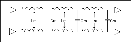
Figure C.16 – Crosstalk coupling mechanisms
These two coupling mechanisms have some interesting characteristics. The polarity of the coupling is opposite for the mutual inductance and coupling capacitance. If the magnitudes of these effects are comparable, then they will cancel, resulting in no forward crosstalk. Unfortunately, accurately computing these values is difficult, and the easiest way to determine the actual amount of crosstalk is to measure it. The other noteworthy characteristic is that the magnitude of the coupled signal is proportional to the rate of change of the signal in the primary line. This is a major reason for controlling the slew rate on ATA bus drivers. Earlier it was said that ringing on the data lines is not necessarily a problem. Here it is seen that fast edge rates and ringing on the data lines can couple by crosstalk into adjacent control lines, causing control sequence errors through mistriggering. It is unlikely crosstalk from data lines causes observable failures in a laboratory environment. But the presence of crosstalk-induced voltage spikes on the control signals reduces the noise margin, and can increase the long-term error rate.
The amplitude of the coupled signal is proportional to the total amount of coupling capacitance and mutual inductance, and is therefore proportional to cable length. Once a line is terminated properly, ringing is no longer a function of length. This leaves crosstalk as the major factor limiting cable length.
Reducing crosstalk involves reducing the mutual inductance, reducing the coupling capacitance, or decreasing the source signal amplitude. Controlling the inductance and capacitance can be done by either keeping the length of the cable short or by increasing the distance between conductors. Placing a ground conductor between critical signals increases the separation of the signals and also adds a shielding effect from the intervening ground. In the ATA environment the only control that can be exercised over the cable is to keep the length at 18 inches or less. The amplitude of the source signal cannot be reduced and still maintain ATA compatibility, but there is control over some elements of the source signal. Slew rate limitation reduces the high-frequency components of the source signal and therefore reduces the coupling of these components into adjacent lines. Terminating the lines reduces ringing which also decreases the amount of energy coupled at the ringing frequency.
- C.4 Bus timing
Terminating the ATA bus has its cost. Partial terminations at the host and the device increase propagation delays throughout the system. The ATA standard specifies that timing is referenced to the input pins of the device (See clause 10). This means that most of the timing issues must be addressed by systems manufacturers and bridge chip designers.
- C.4.1 The issues
The most significant timing issue is the propagation delay of the cable. This needs to be added to the host-side timing. The SPICE model in figure C.17 shows an unterminated host with very fast rise times driving a cable with worst case loads. Two unterminated devices are assumed with the maximum allowed capacitive loading of 25 pF.
Note C.9 - 25 pf was specified in ATA-2.
The simulation results are shown in figure C.18. The period of the ringing is four times the propagation delay of the cable. This simulation shows a cable propagation delay of 5.6 ns. This is twice the value obtained by assuming an 18-inch cable with a propagation velocity of 60% c. The additional delay is due to the presence of the capacitive loads on the cable. This result is important to system designers who take into account worst-case cable delay when specifying the bridge chip timing.
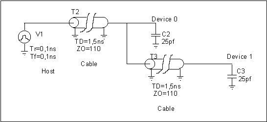
Figure C.17 – SPICE model of ATA cable with worst case loads
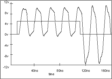
Figure C.18 – Simulation of unterminated ATA cable with worst case loads
From the host point of view, all of the ATA timings are corrected by adding the propagation delay of the cable to insure that the timing is correct at the input pins of the furthest device. Figure C.19 shows a typical corrected result using the read cycle data setup time as an example. The ATA document specifies a setup time at the device of 20 ns (PIO Mode 3). The remaining setup time at the host is only 8,8 ns (20 - 2 x 5,6).
- C.4.2 The influence of termination
If the host has a series partial termination resistor then the bridge chip includes additional timing margin to account for the RC delay of that resistor. Simulations show that the incremental delay added by a series termination resistor at the host is approximately 0,1 ns for a 22 ohm resistor and 1,7 ns for an 82 ohm resistor.
Note C.10 - Assuming Two drive load, 25 pF at each drive, 18-inch cable, 25 pF at host
The extra delay of higher resistor values is one of the reasons that 22 ohm series resistors at the host are recommended.
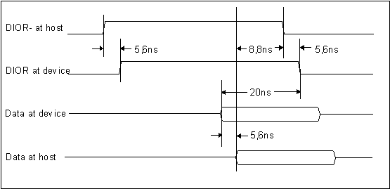
Figure C.19 – Host data setup time during a read cycle
The series resistor at the host is located as close as possible to the ATA connector. To see the importance of this, SPICE simulations are done with the stray capacitance on the driver side of the series resistor and again with the stray capacitance on the cable side. The ringing is reduced when the stray capacitance of the host is on the driver side of the series resistor. A related issue is the distance from the host adapter chip (or chipset) to the ATA connector. Some motherboards have the chip located up to 10 inches away from the connector. This effectively adds another 10 inches to the 18-inch ribbon cable, resulting in an equivalent cable length of 28 inches.
Note C.11 - The traces on the circuit board are from 50 to 200 ohm impedance, so the electrical length of the trace cannot simply be added to the 110 ohm ribbon cable. A SPICE simulation can be used to find the actual delay.
This additional length is not necessarily a problem. If the system manufacturer takes the extra trace delay into account in the application of the host adapter chip, and the total capacitance is kept below the ATA host limit of 25 pF, then in theory there is no difference. Real-world experience indicates that this calculation is rarely done. The distance from the chip to the connector is not addressed in the ATA specification. Keeping the connector within 3 inches (by trace length) of the host adapter chip is recommended.
- C.4.3 Calculating rise time
Chip designers often use a lumped capacitance model for simulating the delay of the output cell. For the simulations this sometimes consists of adding the maximum capacitance allowed for the host and the devices (3 x 25 pF) to an estimated capacitance value for the cable (25 pF). Simulation is then performed with 100 pF capacitance on the output. This does not give an accurate measurement of the timing. A better approximation is to use an output capacitance for the motherboard, a host end termination resistor, and a transmission line to the devices (see figure C.20).
To illustrate how these models are different, suppose that the propagation delay of the output cell simulation is 2 ns too slow. The chip designer (using a 100 pF model) increases the drive current of the output devices. With enough drive current into a purely capacitive load, the 2 ns is removed, bringing the output cell timing back into spec.
Increasing the drive of the output cell in the transmission line model, the length of the cable is not increased and nor increase the speed of signal propagation in the cable is not increased. The 2 ns required time reduction is not achieved by increasing the output drive current. Increasing the output drive current only increases the edge speed, making the ringing worse at the device end (some time is gained with the faster edge speed, but not nearly as much as is predicted with a simple capacitive load model). It is not possible to decrease the overhead by increasing the drive current.
Most ASIC designers find that simulations using the recommended model of figure C.20 show their output cells to be faster than in models with a 100 pF load.
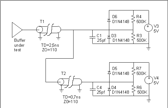
Figure C.20 – Recommended model for I/O cell propagation delay
- C.4.4 Measuring propagation delay
Propagation delay times at the host (and at the device) are measured to the ATA standard of 0,8 V for high to low transitions and 2,0 V for low to high transitions. Many IC manufacturers measure propagation delay at the typical switch point for TTL of 1,4 V. This is not appropriate for the ATA interface since virtually every chip manufacturer (both host and device end) has included hysteresis for noise immunity. Since both the hysteresis window and hysteresis offset of a given receiver move with process, voltage, and temperature, the only guaranteed switch points are the TTL high and low values (0,8 V and 2,0 V).
- C.5 Summary of guidelines
This summary is a collection of reminders for device, system, and chipset designers. They are separated into three groups by relevancy. The guidelines below are not intended to be a strict mandate, but a tool to help everyone build compatible, reliable, high-performance products.
- C.5.1 Guidelines for device designers
·
Terminate signals as shown in table C.1. Consider adding capacitors to ground on these lines if the input capacitance is less than 8 pF, or use active clamping circuits. Place these resistors as close to the ATA connector as possible.
·
Verify that the termination circuit used on received signals has less than 20 pF of equivalent capacitance.
·
Perform a timing analysis to verify that ATA timings are met at the input to the device. Include the time delay due to propagation and cable termination circuits.
- C.5.2 Guidelines for system designers
·
Do not use any value less than 1K ohm for pull up resistors on ATA open-collector signals such as IORDY (as per the standard).
·
The ATA host adapter chip should be located as close as possible to the ATA connector. Keep the trace length between them less than 3 inches.
·
After circuit board fabrication, verify that the total input capacitance at the host is less than 25 pF.
·
Terminate signals as shown in figure C.1. Place these resistors as close to the ATA connector as possible.
·
Perform a system timing analysis to verify that ATA timings are met at the input to the device.
·
For dual port implementations, terminate signals as shown in figure C.15. These resistors should be placed as close to the ATA connector of that port as possible.
·
For dual port implementations, the signal lines CS0- and CS1- should be shared.
·
For dual port implementations, the signal lines DIOR- and DIOW- should not be shared.
·
For dual port implementations, do not share DASP- or PDIAG- signal lines.
·
For dual port implementations, perform a system timing analysis to verify that ATA timings are met at the input of the device. In particular watch the assertion widths of DIOR- and DIOW- to insure that they meet the specification.
·
Route ATA cable away from chassis, power supplies and high speed circuits.
·
Use the shortest cable possiblepractical and never greater than 18 in.
- C.5.3 Guidelines for chip designers