AT Attachment-3 Interface (ATA-3), Revision 6

1-3 Forward, Introduction, Scope, Normative references, Definitions, abbreviations, and conventions
4 Interface physical and electrical requirements
5 Interface signal assignments and descriptions
6 Interface register definitions and descriptions
7 General operational requirements
8 Command descriptions
9 Protocol
10 Timing
Annex A Connectors
Annex B Identify device data for ATA devices below 8 GB
Annex C Signal integrity
Annex D Bibliography
Annex E ATA command set summary


  • Annex A Connectors
  • (normative)

            1. A.1 40-pin connector
            2. The I/O connector is a 40-pin connector as shown in figure A.1, with pin assignments as shown in table A.1. The connector shall be keyed to prevent the possibility of installing it upside down. A key is provided by the removal of pin 20. The corresponding pin on the cable connector shall be plugged.

              The pin locations are governed by the cable plug, not the receptacle. The way in which the receptacle is mounted on the printed circuit board affects the pin positions, and pin 1 shall remain in the same relative position. This means the pin numbers of the receptacle may not reflect the conductor number of the plug. The header receptacle is not polarized, and all the signals are relative to pin 20, which is keyed.

              By using the plug positions as primary, a straight cable can connect devices. As shown in figure A.1, conductor 1 on pin 1 of the plug shall be in the same relative position no matter what the receptacle numbering looks like. If receptacle numbering was followed, the cable would have to twist 180 degrees between a device with top-mounted receptacles, and a device with bottom-mounted receptacles.


              1


              40


              20


              2


              Circuit board


              Circuit board


              1


              40


              20


              2


              Figure A.1 - 40-pin connector mounting

              Table A.1 - 40-pin connector interface signals

              Signal name

              Connector contact

              Conductor

              Connector contact

              Signal name


              RESET-

              1

              1

              2

              2

              Ground

              DD7

              3

              3

              4

              4

              DD8

              DD6

              5

              5

              6

              6

              DD9

              DD5

              7

              7

              8

              8

              DD10

              DD4

              9

              9

              10

              10

              DD11

              DD3

              11

              11

              12

              12

              DD12

              DD2

              13

              13

              14

              14

              DD13

              DD1

              15

              15

              16

              16

              DD14

              DD0

              17

              17

              18

              18

              DD15

              Ground

              19

              19

              20

              20

              (keypin)

              DMARQ

              21

              21

              22

              22

              Ground

              DIOW-

              23

              23

              24

              24

              Ground

              DIOR-

              25

              25

              26

              26

              Ground

              IORDY

              27

              27

              28

              28

              CSEL

              DMACK-

              29

              29

              30

              30

              Ground

              INTRQ

              31

              31

              32

              32

              reserved

              DA1

              33

              33

              34

              34

              PDIAG-

              DA0

              35

              35

              36

              36

              DA2

              CS0-

              37

              37

              38

              38

              CS1-

              DASP-

              39

              39

              40

              40

              Ground

              Recommended part numbers for the mating connector and cable are shown below, but equivalent parts may be used.


              Connector (40 pin)

              3M 3417-7000 or equivalent


              Strain relief

              3M 3448-2040 or equivalent


              Flat cable (stranded 28 AWG)

              3M 3365-40 or equivalent


              Flat cable (stranded 28 AWG)

              3M 3517-40 (shielded) or equivalent


              1. A.1.1 4-pin power connector

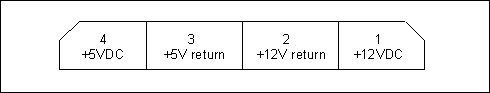
              When the device uses the 40-pin connector, the device receives DC power through a 4-pin connector. The pin assignments are shown in table A.2. Recommended part numbers for the mating connector to 18 AWG cable are shown below, but compatible parts may be used.


              Connector (4 pin)

              AMP 1-480424-0 or compatible


              Contacts (loose piece)

              AMP 60619-4 or compatible


              Contacts (strip)

              AMP 61117-4 or compatible

              Table A.2 - DC interface using 4-pin power connector

              Power line designation

              Pin Number

              +12 Volts

              1

              +12 Volt return

              2

              +5 Volt return

              3

              +5 Volts

              4

              Figure A.2 - Drive side connector pin numbering

            3. A.2 44-pin small form factor connector
            4. This annex describes a connector alternative often used for 2 1/2 inch or smaller devices. This alternative was developed by the Small Form Factor (SFF) Committee, an industry ad hoc group.

              In an effort to broaden the applications for small form factor devices, a group of companies representing system integrators, device suppliers, and component suppliers decided to address the issues involved.

              A primary purpose of the SFF Committee was to define the external dimensions of small form factor devices so that products from different vendors could be used in the same mounting configurations.

              The restricted area and the mating of devices directly to a motherboard required that the number of connectors be reduced, which caused the assignment of additional pins for power. Power is provided to the devices on the same connector as used for the signals, and addresses are set by the receptacle into which the devices are plugged.

              The 50-pin connector that has been widely adopted across industry for SFF devices is a low density 2 mm connector which has no shroud on the plug which is mounted on the device. A number of suppliers provide intermatable components. The following information has been provided to assist users in specifying components used in an implementation.


              Signals Connector Plug

              DuPont 86451 or equivalent


              Signals Connector Receptacle

              DuPont 86455 or equivalent

              1. A.2.1 44-pin signal assignments

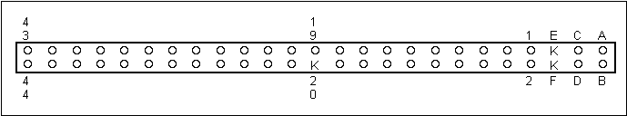
              The signals assigned for 44-pin applications are described in table A.3. Although there are 50 pins in the plug, a 44-pin mating receptacle may be used(the removal of pins E and F provides room for the wall of the receptacle).

              Some devices may utilize pins A, B, C and D for option selection via physical jumpers. Such implementations may require use of the 44-pin receptacle.

              The first four pins of the connector plug located on the device shall not to be connected to the host, as they are reserved for manufacturer's use. Pins E, F and 20 are keys, and are removed. See figure A.3.

              Figure A.3 - 44-pin connector


              Table A.3 - Signal assignments for 44-pin ATA

              Signal name

              Connector contact

              Conductor

              Connector contact

              Signal name

              Vendor specific

              A


              B

              Vendor specific

              Vendor specific

              C


              D

              Vendor specific

              (keypin)

              E


              F

              (keypin)

              RESET-

              1

              1

              2

              2

              Ground

              DD7

              3

              3

              4

              4

              DD8

              DD6

              5

              5

              6

              6

              DD9

              DD5

              7

              7

              8

              8

              DD10

              DD4

              9

              9

              10

              10

              DD11

              DD3

              11

              11

              12

              12

              DD12

              DD2

              13

              13

              14

              14

              DD13

              DD1

              15

              15

              16

              16

              DD14

              DD0

              17

              17

              18

              18

              DD15

              Ground

              19

              19

              20

              20

              (keypin)

              DMARQ

              21

              21

              22

              22

              Ground

              DIOW-

              23

              23

              24

              24

              Ground

              DIOR-

              25

              25

              26

              26

              Ground

              IORDY

              27

              27

              28

              28

              CSEL

              DMACK-

              29

              29

              30

              30

              Ground

              INTRQ

              31

              31

              32

              32

              reserved

              DA1

              33

              33

              34

              34

              PDIAG-

              DA0

              35

              35

              36

              36

              DA2

              CS0-

              37

              37

              38

              38

              CS1-

              DASP-

              39

              39

              40

              40

              Ground

              +5v (logic)

              (see note1)

              41

              41

              42

              42

              +5v (Motor)

              (see note 1)

              Ground(Return)

              (see note1)

              43

              43

              44

              44

              TYPE- (0=ATA)

              (see note 1)

              Note :

              1 Pins which are additional to those of the 40-pin cable.


            5. A.3 68-pin small form factor connector
            6. This subclause defines the pinouts used for the 68-pin alternative connector for the AT Attachment Interface. This connector is the same as the one defined by PCMCIA. This subclause defines a pinout alternative that allows a device to function as an AT Attachment Interface compliant device, while also allowing the device to be compliant with PC Card ATA mode defined by PCMCIA. The signal protocol allows the device to identify the host interface as being 68-pin ATA or PC Card ATA.

              To simplify the implementation of dual-interface devices, the 68-pin AT Attachment Interface maintains commonality with as many PC Card ATA signals as possible, while supporting full command and signal compliance with the ATA standard.

              The 68-pin ATA pinout shall not cause damage or loss of data if a PCMCIA card is accidentally plugged into a host slot supporting this interface. The inversion of the reset signal between the ATA and PCMCIA interfaces prevents loss of data if the device is unable to reconfigure itself to the appropriate host interface.

              1. A.3.1 Signals
              2. This Specification relies upon the electrical and mechanical characteristics of PCMCIA and unless otherwise noted, all signals and registers with the same names as PCMCIA signals and registers have the same meaning as defined in PCMCIA.

                The PC Card-ATA specification is used as a reference to identify the signal protocol used to identify the host interface protocol.

              3. A.3.2 Signal descriptions
              4. Any signals not defined below shall be as described in the ATA, PCMCIA, or the PC Card ATA documents.

                Table A.4 shows the ATA signals and relationships such as direction, as well as providing the signal name of the PCMCIA equivalent.


                Table A.4 - Signal assignments for 68-pin ATA

                Pin

                Signal

                Hst

                Dir

                Dev

                PCMCIA


                Pin

                Signal

                Hst

                Dir

                Dev

                PCMCIA

                1

                Ground

                x

                ®

                x

                Ground


                35

                Ground

                x

                ®

                x

                Ground

                2

                DD3

                x

                «

                x

                D3


                36

                CD1-

                x

                ¬

                x

                CD1-

                3

                DD4

                x

                «

                x

                D4


                37

                DD11

                x

                «

                x

                D11

                4

                DD5

                x

                «

                x

                D5


                38

                DD12

                x

                «

                x

                D12

                5

                DD6

                x

                «

                x

                D6


                39

                DD13

                x

                «

                x

                D13

                6

                DD7

                x

                «

                x

                D7


                40

                DD14

                x

                «

                x

                D14

                7

                CS0-

                x

                ®

                x

                CE1-


                41

                DD15

                x

                «

                x

                D15

                8


                ®

                i

                A10


                42

                CS1-

                x

                ®

                x(1)

                CE2-

                9

                SELATA-

                x

                ®

                x

                OE-


                43


                ¬

                i

                VS1-

                10


                44

                DIOR-

                x

                ®

                x

                IORD-

                11

                CS1-

                x

                ®

                x(1)

                A9


                45

                DIOW-

                x

                ®

                x

                IOWR-

                12


                ®

                i

                A8


                46


                13


                47


                14


                48


                15


                ®

                i

                WE-


                49


                16

                INTRQ

                x

                ¬

                x

                READY/

                IREQ-


                50


                17

                Vcc

                x

                ®

                x

                Vcc


                51

                Vcc

                x

                ®

                x

                Vcc

                18


                52


                19


                53


                20


                54


                21


                55

                M/S-

                x

                ®

                x(2)


                22


                ®

                i

                A7


                56

                CSEL

                x

                ®

                x(2)


                23


                ®

                i

                A6


                57


                ¬

                i

                VS2-

                24


                ®

                i

                A5


                58

                RESET-

                x

                ®

                x

                RESET

                25


                ®

                i

                A4


                59

                IORDY

                o

                ¬

                x(3)

                WAIT-

                26


                ®

                i

                A3


                60

                DMARQ

                o

                ¬

                x(3)

                INPACK-

                27

                DA2

                x

                ®

                x

                A2


                61

                DMACK-

                o

                ®

                o

                REG-

                28

                DA1

                x

                ®

                x

                A1


                62

                DASP-

                x

                «

                x

                BVD2/

                SPKR-

                29

                DA0

                x

                ®

                x

                A0


                63

                PDIAG-

                x

                «

                x

                BVD1/

                STSCHG

                30

                DD0

                x

                «

                x

                D0


                64

                DD8

                x

                «

                x

                D8

                31

                DD1

                x

                «

                x

                D1


                65

                DD9

                x

                «

                x

                D9

                32

                DD2

                x

                «

                x

                D2


                66

                DD10

                x

                «

                x

                D10

                33


                x

                ¬

                x

                WP/

                IOIS16


                67

                CD2-

                x

                ¬

                x

                CD2-

                34

                Ground

                x

                ®

                x

                Ground


                68

                Ground

                x

                ®

                x

                Ground

                Key:

                Dir = the direction of the signal between host and device.

                x in the Hst column = this signal shall be supported by the Host.

                x in the Dev column = this signal shall be supported by the device.

                i in the Dev column = this signal shall be ignored by the device while in 68-pin ATA mode.

                o = this signal is Optional.

                Nothing in Dev column = no connection should be made to that pin.

                Notes:

                1 The device shall support only one CS1- signal pin.

                2 The device shall support either M/S- or CSEL but not both.

                3 The device shall hold this signal negated if it does not support the function.


              5. A.3.2.1 CD1- (Card Detect 1)
              6. This signal shall be grounded by the device. CD1- and CD2- are used by the host to detect the presence of the device.

              7. A.3.2.2 CD2- (Card Detect 2)
              8. This signal shall be grounded by the device. CD1- and CD2- are used by the host to detect the presence of the device.

              9. A.3.2.3 CS1- (Device chip select 1)
              10. Hosts shall provide CS1- on both the pins identified in table A.4.

                Devices shall recognize only one of the two pins as CS1-.

              11. A.3.2.4 DMACK- (DMA acknowledge)
              12. This signal is optional for hosts and devices.

                If this signal is supported by the host or the device, the function of DMARQ shall also be supported.

              13. A.3.2.5 DMARQ (DMA request)
              14. This signal is optional for hosts.

                If this signal is supported by the host or the device, the function of DMACK- shall also be supported.

              15. A.3.2.6 IORDY (I/O channel ready)
              16. This signal is optional for hosts.

              17. A.3.2.7 M/S- (Master/slave)
              18. This signal is the inverted form of CSEL. Hosts shall support both M/S- and CSEL though devices need only support one or the other.

                Hosts shall assert CSEL and M/S- prior to applying VCC to the connector.

              19. A.3.2.8 SELATA- (Select 68-pin ATA)
              20. This pin is used by the host to select which mode to use, PC Card-ATA mode or the 68-pin ATA mode. To select 68-pin ATA mode, the host shall assert SELATA- prior to applying power to the connector, and shall hold SELATA- asserted.

                The device shall not re-sample SELATA- as a result of either a Hard or Soft Reset. The device shall ignore all interface signals for 19 ms after the host supplies Vcc within the device's voltage tolerance. If SELATA- is negated following this time, the device shall either configure itself for PC Card-ATA mode or not respond to further inputs from the host.

              21. A.3.3 Removability considerations
              22. This Specification supports the removability of devices which use the ATA protocol. As removability is a new consideration for ATA devices, several issues need to be considered with regard to the insertion or removal of devices.

              23. A.3.3.1 Device recommendations

    The following are recommendations to device implementors:

                1. A.3.3.2 Host recommendations

    The following are recommendations to host implementors: