Connectors are documented in Annex A.
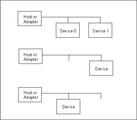
This standard defines the ATA interface containing a single host or host adapter and one or two devices. If two devices are connected to the interface, they are connected in a daisy chained configuration. One device is configured as Device 0 and the other device as Device 1.
The designation of a device as Device 0 or Device 1 may be made in a number of ways:
In a two drive configuration, a device shall be at one end of the ATA interface cable and the host shall be placed at one end of the cable.
It should be recognized that if a single device is configured at the end of the cable using CSEL, a device 1 only configuration will results. If a single device configuration is implemented with the device in the middle, a cable stub results that may cause degredation of signals. Also see 5.2.15.
Figure 1- ATA interface cabling diagram
The cable specification affects system integrity and the maximum length that can be supported in any application.
Cable total length shall not exceed 0,46 m (18 in).
Cable capacitance shall not exceed 35 pf.
Interface signals are defined in Table 2 and Table 3.
|
Description |
Min |
Max |
|
|
IoL |
Driver sink current (See note 1) |
4 mA |
|
|
IoH |
Driver source current (See note 2) |
400 m A |
|
|
ViH |
Voltage input high |
2,0 V D.C. |
|
|
ViL |
Voltage input low |
0,8 V D.C. |
|
|
VoH |
Voltage output high (IoH = -400 m A) |
2,4 V D.C. |
|
|
VoL |
Voltage output low (IoL = 12 ma) |
0,5 V D.C. |
|
|
Notes: 1 IoL for DASP shall be 12 mA minimum to meet legacy timing and signal integrity. 2 IoH value at 400 m A is insufficient in the case of DMARQ which is typically pulled low by a 5,6 kW resistor. |
|||
|
Description |
Min |
Max |
|
|
tRISE |
Rise time for any signal on AT interface (See note 1) |
5 ns |
|
|
tFALL |
Fall time for any signal on AT interface (See note 1) |
5 ns |
|
|
Cin |
Host input capacitance |
25 pf |
|
|
Cout |
Host output capacitance |
25 pf |
|
|
Cin |
Device input capacitance |
20 pf |
|
|
Cout |
Device output capacitance |
20 pf |
|
|
Note: 1 tRISE and tFALL are measured from 10-90% of full signal amplitude with a total capacitive load of 40 pf. |
|||
Table 4 - Driver types and required pull-ups
|
Signal |
Source |
Driver type (see note 1) |
Pull-up at host (see note 2) |
Pull-up at each device (see note 2) |
Notes |
|
|
Reset |
Host |
TP |
||||
|
DD (15:0) |
Bidir |
TS |
3 |
|||
|
DMARQ |
Device |
TS |
5,6 kW PD |
4 |
||
|
DIOR- DIOW- |
Host |
TS |
||||
|
IORDY |
Device |
TS |
1,0 kW |
5 |
||
|
CSEL |
Host |
Ground |
10 kW |
6 |
||
|
DMACK- |
Host |
TP |
||||
|
INTRQ |
Device |
TS |
||||
|
DA (2:0) |
Host |
TP |
||||
|
PDIAG- |
Device |
TS |
10 kW |
|||
|
CS0- CS1- |
Host |
TP |
||||
|
DASP- |
Device |
OC |
10 kW |
|||
|
Notes: 1 TS=Tri-state; OC=Open Collector; TP=Totem-pole; PU=Pull-up; PD=Pull-down; VS=Vendor specific 2 All resistor values are minimum (lowest) allowed. 3 Devices shall not have a pull-up resistor on DD7. It is recommended that a host have a 10 kW pull-down resistor and not a pull-up resistor on DD7 to allow a host to recognize the absence of a device at power-up. It is intended that this recommendation become mandatory in a future revision of this standard. 4 ATA-3 defines this line to be tri-stated whenever the device is not selected or is not executing a DMA data transfer. When enabled by DMA transfer, it shall be driven high and low by the device. 5 This signal should only be enabled during DIOR/DIOW cycles to the selected device. 6 When used as CSEL, this line is grounded at the Host and a 10 kW pull-up is required at both devices. |
||||||