The physical interface consists of receivers and drivers communicating through a set of conductors using an asynchronous interface protocol. Signal names are shown in Table 5. For connector descriptions see Annex A.
Table 5 - Interface signal name assignments
|
Description |
Host |
Dir |
Dev |
Acronym |
|
Cable select |
(See note 1) |
CSEL |
||
|
Chip select 0 |
® |
CS0- |
||
|
Chip select 1 |
® |
CS1- |
||
|
Data bus bit 0 |
« |
DD0 |
||
|
Data bus bit 1 |
« |
DD1 |
||
|
Data bus bit 2 |
« |
DD2 |
||
|
Data bus bit 3 |
« |
DD3 |
||
|
Data bus bit 4 |
« |
DD4 |
||
|
Data bus bit 5 |
« |
DD5 |
||
|
Data bus bit 6 |
« |
DD6 |
||
|
Data bus bit 7 |
« |
DD7 |
||
|
Data bus bit 8 |
« |
DD8 |
||
|
Data bus bit 9 |
« |
DD9 |
||
|
Data bus bit 10 |
« |
DD10 |
||
|
Data bus bit 11 |
« |
DD11 |
||
|
Data bus bit 12 |
« |
DD12 |
||
|
Data bus bit 13 |
« |
DD13 |
||
|
Data bus bit 14 |
« |
DD14 |
||
|
Data bus bit 15 |
« |
DD15 |
||
|
Device active or slave (device 1) present |
(See note 1) |
DASP- |
||
|
Device address bit 0 |
® |
DA0 |
||
|
Device address bit 1 |
® |
DA1 |
||
|
Device address bit 2 |
® |
DA2 |
||
|
DMA acknowledge |
® |
DMACK- |
||
|
DMA request |
¬ |
DMARQ |
||
|
Interrupt request |
¬ |
INTRQ |
||
|
I/O read |
® |
DIOR- |
||
|
I/O ready |
¬ |
IORDY |
||
|
I/O write |
® |
DIOW- |
||
|
Passed diagnostics |
(See note 1) |
PDIAG- |
||
|
Reset |
® |
RESET- |
||
|
Note: 1 See signal descriptions for information on source of these signals |
||||
This is the chip select signal from the host used to select the Command Block registers. See Table 6.
This is the chip select signal from the host used to select the Control Block registers. See Table 6.
This is the 3-bit binary coded address asserted by the host to access a register or data port in the device. See Table 6.
This is a time-multiplexed signal which indicates that a device is active, or that Device 1 is present. This signal shall be an open collector output and each device shall have a 10 kW pull-up resistor.
If the host connects to the DASP- signal for the illumination of an LED or for any other purpose, the host shall ensure that the signal level seen on the ATA interface for DASP- shall maintain VoH and VoL compatibility, given the IoH and IoL requirements of the DASP- device drivers.
This is an 8- or 16-bit bi-directional data interface between the host and the device. The lower 8 bits are used for 8-bit register transfers.
This is the read strobe signal from the host. The falling edge of DIOR- enables data from the device onto the signals, DD (7:0) or DD (15:0). The rising edge of DIOR- latches data at the host and the host shall not act on the data until it is latched.
This is the Write strobe signal from the host. The rising edge of DIOW- latches data from the signals, DD (7:0) or DD (15:0), into the device. The device shall not act on the data until it is latched.
This signal shall be used by the host in response to DMARQ to initiate DMA transfers.
This signal, used for DMA data transfers between host and device, shall be asserted by the device when it is ready to transfer data to or from the host. The direction of data transfer is controlled by DIOR- and DIOW-. This signal is used in a handshake manner with DMACK- i.e., the device shall wait until the host asserts DMACK- before negating DMARQ, and re-asserting DMARQ if there is more data to transfer.
This line shall be released (high impedance state) whenever the device is not selected or is selected and no DMA command is in progress. When enabled by DMA transfer, it shall be driven high and low by the device.
When a DMA operation is enabled, CS0- and CS1- shall not be asserted and transfers shall be 16-bits wide.
This signal is used to interrupt the host system. INTRQ is asserted only when the device has a pending interrupt, the device is selected, and the host has cleared the nIEN bit in the Device Control register. If the nIEN bit is equal to one, or the device is not selected, this output is in a high impedance state, regardless of the presence or absence of a pending interrupt.
The pending interrupt condition shall be set by:
The pending interrupt condition shall be cleared by:
Obsolete.
This signal is negated to extend the host transfer cycle of any host register access (Read or Write) when the device is not ready to respond to a data transfer request.
If actively asserted, this signal shall only be enabled during DIOR-/DIOW- cycles to the selected device. If open collector, when IORDY is not negated, it shall be in the high-impedance (undriven) state.
The use of IORDY is required for PIO modes 3 and above and otherwise optional.
This signal shall be asserted by Device 1 to indicate to Device 0 that it has completed diagnostics. A 10 kW pull-up resistor shall be used on this signal by each device.
The host shall not connect to the PDIAG- signal.
This signal from the host system shall be asserted beginning with the application of power and held asserted until at least 25 m s after voltage levels have stabilized within tolerance during power on and negated thereafter unless some event requires that the device(s) be reset following power on.
ATA devices shall not recognize a signal assertion shorter than 20 ns as a valid reset signal. Devices may respond to any signal assertion greater than 20 ns, and shall recognize a signal equal to or greater than 25 m s.
This signal shall have a 10 kW pull-up resistor at each device.
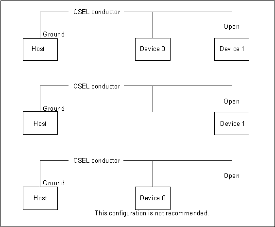
The device is configured as either Device 0 or Device 1 depending upon the value of CSEL:
CSEL shall be maintained at a steady level for at least 31 s after the negation of RESET-.
Note 3: Special cabling can be used by the system manufacturer to selectively ground CSEL e.g., CSEL of Device 0 is connected to the CSEL conductor in the cable, and is grounded, thus allowing the device to recognize itself as Device 0. CSEL of Device 1 is not connected to CSEL because the conductor is removed, thus the device can recognize itself as Device 1.
Figure 2 - Cable select example