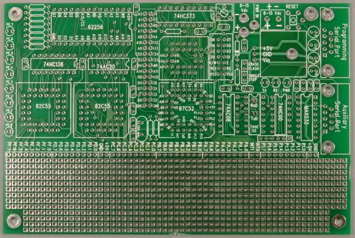
Bare Circuit Board for the 8051 Development Board
| Sold Out | DEV_PCB_BARE | Bare Circuit Board for the 8051 Development Board | $25 |
|
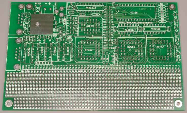
The 8051 development board provides an easy and low-cost way to develop your 8051 based microcontroller projects, without purchasing any other equipment, such as IC programmers or emulators. The board is intended to be used with an 87C52 chip loaded with PAULMON2 (available separately), which provides a simple menu-based system that enables you to download your own code into the RAM or Flash ROM (not provided with the bare board) . When your project is finished, you can set a few bytes to tell PAULMON2 to automatically run your program at start-up, and download it into the Flash ROM chip, so the board will then run your application instead of booting into the PAULMON2 menu system. Should you need to erase the Flash ROM to make changes, a pair of pads intended for a jumper may be shorted to cause PAULMON2 to erase the Flash ROM chip.
The board supports two 82C55 chips (not provided with the bare board), that can provide 40 I/O lines and 8 LEDs, in addition to the 10 lines from the 8051's port #1, and the 8051's bus lines. A location for a second serial connector is available, with a simple switching circuit, to make it easier to develop applications that need the serial port and must not see the menus from PAULMON2. The bottom section of the board is a pad-per-hole prototype area, where simple circuits can be added.
The bare board includes no other components, only the circuit board. The board is a professional quality board, with plate-through holes, green solder mask, and a silk screen to make loading the components easier.
The back side of this board also includes extensive legend markings to label important signals and components. This back side lettering makes modifications and construction in the prototype area much easier.
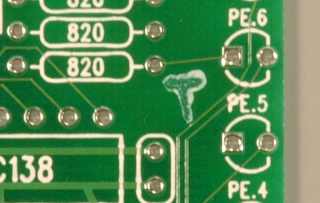
PJRC pays the circuit board fabricator to electrically test all of these boards. Every board is placed on a test fixture that makes contact will all the holes (except for the prototype area) and it verifies the connectivity of all the traces. When the boards that pass this test have a small "T" marking added, as show in this photo: