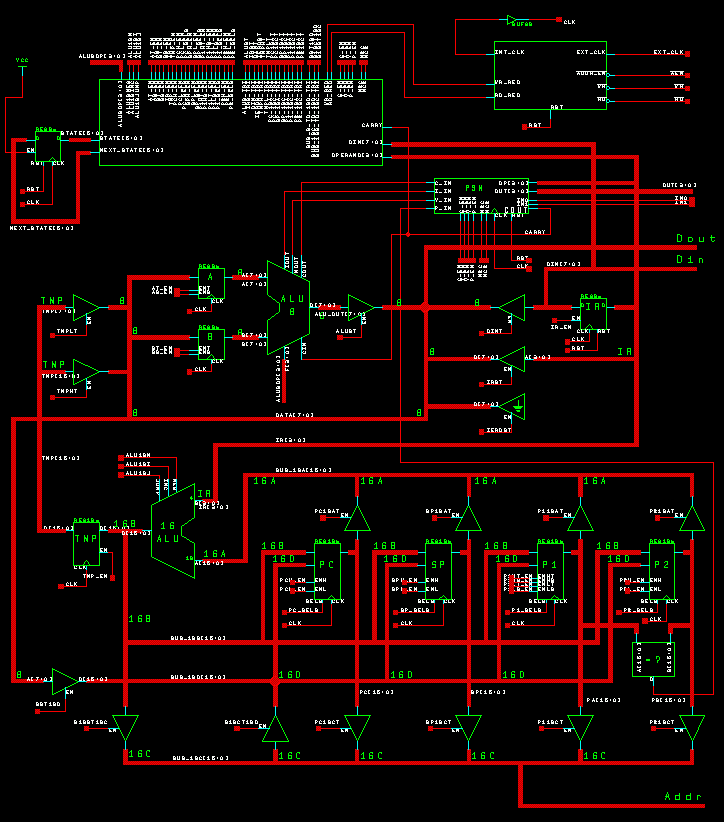
skip navigational linksPJRC
Shopping Cart Download Website
Home Products Teensy Blog Forum
You are here: OSU8 Microprocessor Schematic OSU8 Core Normal Size

OSU8 Microprocessor
Overview
CPU Programming
Hardware Info
Schematic
Implementation
Download Files

OSU8 Core Schematic

This is the main schematic for OSU8, which contains the complete top-level view of the data paths, registers, logic and buffers. Please refer to the detailed description of the OSU8 Data Path, for a description of how this circuitry is used to implement the processors instructions.

Thoughout these schematics, the green blocks are links to their lower level schematics. Individual gates and flip-flops do not have schematics under them, because they are the primitive elements for Xilinx place-and-route, and for the ViewSim gate-level simulation.

Also, view a much larger and more readable version

Lower Schematics

Schematic Drawing Control State Register Control Logic Bus Control Status Bits Tri-State Buffer Tri-State Buffer A Register B Register 8-bit ALU, All Data Operations Tri-State Buffer Tri-State Buffer Tri-State Buffer Tri-State Pulldown Current Operand Register Temporary Storage Register 16-bit ALU, Address Computations Tri-State Buffer Tri-State Buffer Tri-State Buffer Tri-State Buffer Program Counter Stack Pointer P1 Pointer Register P2 Pointer Register 16-bit Equality Compare Tri-State Buffer Tri-State Buffer Tri-State Buffer Tri-State Buffer Tri-State Buffer Tri-State Buffer Tri-State Buffer


OSU8: Simple 8-Bit Microprocessor Design; Paul Stoffregen
http://www.pjrc.com/tech/osu8/sch/osu8.html
Last updated: February 24, 2005
Status: These pages are a work-in-progress
Comments, Suggestions: <paul@pjrc.com>