|
|
| ||
|
Shopping Cart
|
| Home | Products | Teensy | Blog | Forum |
|
You are here:
OSU8 Microprocessor
|
|
|
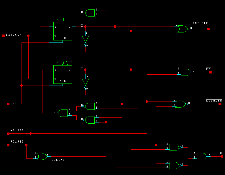
Bus ControllerThis small state machines is a simple bus controller. The EXT_CLK signal is the external clock signal from the circuit board, and INT_CLK is the clock that drive OSU8's core circuitry. The internal circuitry is clocked at 1/4 of the extrnal clock speed, so that the bus controller can assert signals on the bus with timing that will work for standard external EPROM and SRAM chips.The control section asserts either RD_REQ or WR_REQ, and causes the desired address to appear on bus 16C. For a read request, OSU8's core expects valid data to be present on the Din bus at the next rising edge of the internal clock. For a write request, the data on the Dout bus must have been properly stored before the next rising edge of the internal clock. This simple state machine has 4 external clock cycles to accomplish those tasks. This simple circuit falls far short of optimizing OSU8's speed, because it breaks the bus cycle into four timing periods, of equal length, during which time only one internal machine cycle is executed. A better bus controller could be designed, to improve OSU8's performance. At the very least, it could use "half cycles" to allow more of the time for the external memory's access time, which probably allow a faster clock.
|