|
|
Original Project Specification
The original document written by Richard Schreier is available in
Postscript format. This web page is
more or less similar to the original specification
distributed in January 1993.
Important Information
Timetable: TIGHT!
- The layout is due Monday March 1 at 9:30am.
- The project report is due March 5 at 5:00pm.
- The assignments during the term are geared toward helping
you to complete the project on time. It is in your best interest
to keep pace with them.
General Information:
- Chip design will be done in pairs.
- For each design, MOSIS will give us 4 parts, but I will
keep at least 1 from each group. The rest are yours.
- The chip is 2.2x2.2mm (a MOSIS TinyChip) and will be in a 28-pin DIP.
- The process is a 2.0m P-well, double-poly process.
- Vineet will provide the basic pad frame.
- You can (and should) use cells from the CMOSN library whenever possible.
Project Contents:
- Your IC will contain a ring-oscillator with divide-by-32
circuitry, an RS latch (which you can use to generate a glitch-free
clock during manual testing) and a decimator for a multi-bit
delta-sigma modulator. Design of the decimator will constitute
the major portion of the project. Detailed specifications for
the decimator are given in the remainder of this handout. You
should be aware that the specifications will likely change as
you discover how difficult it is to squeeze all the customer's
features into one TinyChip.
Project Evaluation:
- Vineet will check the layout for DRC errors. There should be none.
The bulk of the marks will be based on the report. I expect to see
- A description of the function and I/O timing of your chip.
- A plot of your chip and of the major cells.
- Schematics of the cells used, annotated with transistor sizes.
- Simulations and calculations. (Estimated ring-oscillator
oscillation frequency, maximum clock speed, clock-buffer
calculations etc.)
- A description of what you did with your left-over area
(if anything) and relevant calculations.
Free Space:
- If there is free space, you may put anything you like in it.
The fact that this is a double-poly process implies that you can
implement analog functions using switched-capacitor circuits.
Ring Oscillator:
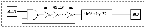
Figure 1: When REN is high, the ring oscillator should
oscillate, and its divided-down output should be available at RO.
RS Latch:
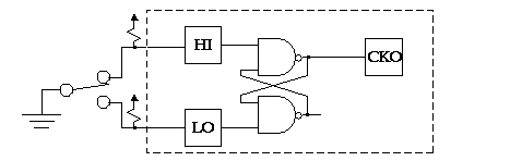
Figure 2:An external toggle switch can be used to
generate a glitch-free clock signal at CKO. This can be
helpful during manual testing.
Decimator: General Information
The main function of the chip is to act as a decimator for a
multi-bit delta-sigma modulator. Don't worry if you don't understand
the purpose of this block; you only need to understand its operation
well enough to build it.
Figure 3 shows the block diagram of the decimator using digital
signal processing (DSP) notation. If you don't know what represents,
don't panic; you can view the formulae in the boxes simply as
names. What you should observe from FigureĀ3 is that the incoming
data, x, is passed through four identical blocks, then sub-sampled
and passed through another four identical blocks to produce the
output y. An alternative specification for the decimator is given
in Figure 4, which specifies the operations of the decimator are
with a C program.
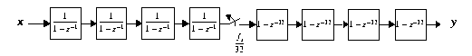
Figure 3:The block diagram of the decimator in DSP notation.
Note: This C code is available
plain
or in
ZIP
format.
/*
 * decimate.c
 * Simulate the mathematical operations carried out
 * by a sinc^4 decimator with a decimation factor of 32.
 *
 * The decimator uses modulo 2^24 arithmetic to do
 * its calculations.
 *
 * R. Schreier of OSU, 1993.
 */

#define R 32
#define N 24

static int Modulus = 1<<N;
static int Signbit = 1<<(N-1);
static int Mask = (1<<N)-1;

int mod( int x ){
    return x&Mask;
    }

main(){
/* Declarations. */
int a1=0, a2=0, a3=0, a4=0, s1=0, s2=0, s3=0, s4=0;
int t, x, y1, y2, y3, y4;

/*
printf("Signbit = %.8x\n", Signbit );
printf("Mask = %.8x\n", Mask );
*/

/* Get the input and go through the equations. */
for(t=0; scanf("%d",&x) > 0; ){
    a1 = mod( a1 + x );
    a2 = mod( a2 + a1 );
    a3 = mod( a3 + a2 );
    a4 = mod( a4 + a3 );
    if( ++t == R ){
        t = 0;
        y1 = mod( a4 - s1 );
        s1 = a4;
        y2 = mod( y1 - s2 );
        s2 = y1;
        y3 = mod( y2 - s3 );
        s3 = y2;
        y4 = mod( y3 - s4 );
        s4 = y3;
        if( y4 & Signbit )
            printf( "%d\n", y4 - Modulus );
        else
            printf( "%d\n", y4 );
        }
    }
exit(0);
}
Figure 4:A C program which simulates the operation of the
decimator. Source is available in ~schreier/ece517/decimate.c and
the executable is decimate, in the same directory.
As your customer, I want the chip to accept data at a frequency of at
least 10ĀMHz. For an input data width of 4 bits, I have determined
that the internal data path needs to be 24 bits wide. If you can
increase the internal word width, then the input data width can be
increased and I will be happier. Six pins have therefore been
allocated for the input data, even though I expect that you will
only be able to accommodate four (or fewer). See Table 1 for a list
of the pins and their functions.
Note that pins 12-18 have not been assigned. I expect that you will
want to omit them, so as to give yourself more space on the IC for
gates. See FigureĀ5 for the pad layout that was used last year. If
you can cram all the functions I want into 1700l X 1700l, then you
can add pads to give yourself more free pins. At the moment, only
pin 26 is free, and I have specified it as an output. Vineet will
issue more details on the pad frame when he finishes laying it out.
The output of the decimator is a 24-bit word, which will be output
serially through the Y pin, with the LSB coming out first. To
demarcate words, FS (frame sync) will be high when the LSB appears
and low otherwise. The OK output is to be asserted at the end of
the automatic self-test, which is initiated by TM (test mode) going
high. Transitions on TM should reset the IC.
| Number |
Type |
Name |
Block |
Number |
Type |
Name |
Block |
| 1 |
Input |
REN |
Ring Osc. |
15 |
| 2 |
Input |
X0(lsb) |
Decimator |
16 |
| 3 |
Input |
X1 |
Decimator |
17 |
| 4 |
Input |
X2 |
Decimator |
18 |
| 5 |
Input |
X3 |
Decimator |
19 |
Output |
CKO |
RS Latch |
| 6 |
Input |
X4 |
Decimator |
20 |
Input |
HI |
RS Latch |
| 7 |
Input |
X5 |
Decimator |
21 |
Input |
LO |
RS Latch |
| 8 |
VDD |
VDD |
|
22 |
VDD |
VDD |
| 9 |
VSS |
VSS |
|
23 |
VSS |
VSS |
| 10 |
Input |
CK |
Decimator |
24 |
Output |
Y |
Decimator |
| 11 |
Input |
TM |
Testing |
25 |
Output |
FS |
Decimator |
| 12 |
|
|
|
26 |
Output |
Spare |
Spare |
| 13 |
|
|
|
27 |
Output |
OK |
Testing |
| 14 |
|
|
|
28 |
Output |
RO |
Ring Osc. |
Table 1: Pin Data
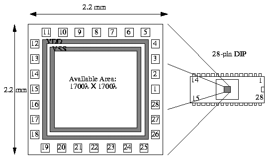
Figure 5:The placement of a TinyChip inside a 28 pin DIP. Pins 12-18 may be omitted to increase the area available for gates.
Decimator:
 block
block
This block, which I shall refer to as the summer block, produces
as its output the sum of all previous inputs. It works by keeping
a running total of its input and adding successive inputs to the
running total. See FigureĀ6 for a digital-logic representation
of the required function. The variables a1, a2, a3 and a4 in the
C program represent the running totals of the four integrator
blocks. Note that for correct operation of this block, the adder
must "roll-over" when overflows occur. This is modelled in the C
program by a modulo 224 operation on all variables. This operation
guarantees that the integers in the C program contain at most 24 bits.
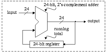
Figure 6: The logic required for the summer block.
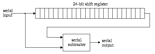
Figure 7:Logic implementation of the subtracter block.
Decimator:
 block
block
The first block you will design (for Assignment 2) is the,
or subtracter, block. This block produces as its output the
difference between its two most recent inputs. Since the sample
rate for the subtracters is of the sample rate for the summers,
you can save hardware by making this block operate serially.
FigureĀ7 gives a hint as to how you might implement the subtracter.
It is up to you to determine the contents of the block labelled
"serial subtracter".
In the C program, the variables s1, s2, s3 and s4 contain the
values in the subtracter register and the variables y1, y2, y3
and y4 are the four subtracter outputs. Your design must operate
in a manner that is consistent with the operation specified in
the C program. (You should use the program to generate test data.)
Be careful to reset the state of the serial subtracter before each cycle.
Decimator: Test mode
To make testing of your IC trivial, I would like it to contain
built-in self-test (BIST) circuitry. We will cover this later
in the course. The idea in a nutshell is to supply a known set
of pseudo-random inputs to the circuit for many clock cycles, do
signature analysis on the output and compare the results with what
you get from simulating a functional circuit. This explains why you
have to put the IC into a known state before proceeding with the
self-test.
To whet your appetite, the input generation and output distillation
are both done with linear-feedback shift registers (LFSRs). The clock
signal can be supplied externally, but if you like you can use the
ring oscillator to supply a clock signal, and thus have a totally
automatic self-test.
|