|
|
| ||
|
Shopping Cart
|
| Home | Products | Teensy | Blog | Forum |
|
You are here:
8051 Tools
|
|
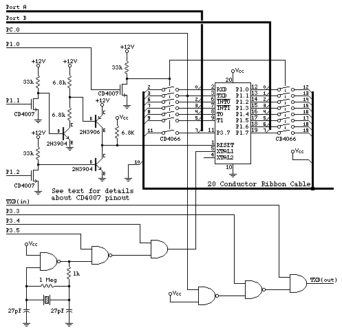
Atmel 89C2051 In-Circuit Programmer SchematicThis is a "beta release" schematic. Use at your own risk The idea is to add this circuitry to a board with already has ram at 2000 and an 82C55 I/O chip to provide ports A, B and C.Warning: not shown here is a memory mapping trick which is described below. You must figure out a way to provide the necessary memory mapping to make beta version 0.003 work. The next beta release will fix this problem, so that an ordinary memory configuration will work... but for now a hardware trick or some preprocessing of your intel hex files is needed.
The AND and NAND gates shown should be 74HC08 and 74HC00
respectively. It a TTL type NAND gate is used (eg LS, L, S, ALS, etc)
the crystal oscillator may be problematic.
Several people have asked how to save images. Here's a few things to try. NOTE: in the above schematic, the line indicated P3.3 (which controls the TXD echo feature) should really connect to P3.4, and the one labeled P3.4 really ought to connect to P3.3. Sorry... I'll get a fixed copy of this schematic on-line sometime, with the signals names that now appear in BETA Version 0.004. On the bright side, if you do connect it differently, it's a simple matter to reassign the pins in the software with 0.004. The inputs on the left side of the schematic come from the ports on the 8051 and 82C55. Port A, Port B, and PC.0 come from the 82C55, and the other lines are from the 8051. The TXD pin of the 8051 is connected to the TXD(in) input line, and the TXD(out) line is connected to the line driver for the programmer's serial transmit. This simple three gate circuit provides the "echo-through" feature which is useful for troubleshooting code while the 89C2051 is in-circuit by echoing data to the programmer's transmit line. The 20 pin ribbon cable should leave pins 1, 4, and 5 unconnected. Double check that pin 10 is connected to ground. add stuff here about the power supply issues. I suggest connecting pin 20 in the ribbon cable to Vcc on the programmer... Do not connect XTAL2 (pin 4) of the 89C2051 chip. The 15 switches shown are the gates within the CD4066, so four of these chips are required. The three NMOS transistors are within a single CD4007 chip. The trick here is to not use the three PMOS transistors which also come in this chip. You must connect +12 volts to pin 14. I'll add more more detailed information about how to connect this chip, hopefully in a week or so. let me know if you're building from this beta schematic and need some assistance. Basically, the two PMOS transistors with floating drains get their drains and sources connected to Vcc. The third PMOS transistor whose drain is connected to an NMOS drain inside the chip gets it's source (the other line) connected to the drain, which is also the drain of one of the NMOS transistors. Pin 14 MUST be connected to +12 volts to avoid damage to this chip. Warning: beta code 0.003 expects RAM to exist at location 0x2000 to store a copy of the data to be programmed into the 89C2051. The code for the 89C2051 must be assembled at location 0000. Beta version 0.003 uses the download code from the unreleased version of paulmon2, without any modification. When you download the code, beginning at location 0000, it really needs to get stored at location 2000, and so on. To accomplish this, I just AND'd the Y0 and Y1 lines from the 74HC138 chip. However, for the development board example, this prevents the EPROM from working. I used the built-in EPROM in an 87C51 for the first version of this project, so this isn't a problem. If you have an 87C51 and a programmer for it, this is the easiest way to make it work. For now, beta version 0.003 requires some sort of hardware trick so writes to 0000 go into 2000, and so on. An alternate workaround is to assemble at 0000 and then modify the intel hex code to shift everything to location 2000, so that the download code will just write the data where the programmer needs it to be. Here is some C source code to read and write intel hex files, if you want to take this approach. This isn't a problem with BETA version 0.004 since 0.004 does address translation in software. All you have to do is specify the physical location of the buffer memory near the top of the program (in an .equ line), reassemble (as31 works), and 0.004 will use this buffer memory when the user tries to download/upload/view code assembled starting at 0000. As well, you're not limited to having the buffer at 2000 with 0.004, you can specify it's location. I wasn't too careful about using MOVX or MOVC to read external memory... my board has the AND gate to combine the two memory spaces. A future release will use MOVC exclusively, but I believe version 0.003 uses MOVX quite a bit. Version 0.004 uses MOVX to read from the buffer memory... maybe MOVC here and there as well. |