| PJRC Home | MP3 Player | 8051 Tools | All Projects | PJRC Store | My Order | Site Map |
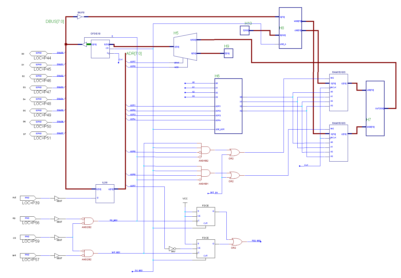
Not shown here (it's on another sheet), is a small state machine which controls what the hard is doing. Currently it only has two states (on flip-flop). The states are idle and DO_8051.
The two FDCE flip-flops near the bottom make a single request to the state machine, whenever the 8051 begins a bus cycle. The state machine must always respond within three clock cycles to meet the 8051's timing requirements, fortunately it will always respond on the next cycle. During a 8051 cycle, the DO_8051 signal is asserted, which causes the OFDEX8 flip-flop to obtain whatever located was requested, and if the 8051 bus cycle is a write, one of the WE pins on the RAM is driven to cause the RAM to be updated at the end of the cycle.
The RAM is 16 bits wide, as the planned circuitry (not drawn yet) processes everything 16 bits at a time. The two blocks labeled H9 and H10 are dummy signals, where data to/from the DRAM, IDE interface, and a shift register to the MP3 decoder will be connected. The H6 block allows the 8051 address to control the RAM's address pins during a 8051 cycle, but at all other times the state machine has direct control over the RAM address.
The rough plan is to dedicate various RAM addresses to certain tasks. For example, for read/write to the DRAM, three 16-bit addresses will be dedicated. The 8051 will write 4 bytes for the desired address, and for writes also 2 bytes of data. For reads, it will read the two bytes. Not drawn yet are status bits and a command register, that will turn 8051 bus cycles into a set of request bits, similar to the DO_8051 shown here.
Well, that's enough rambling.... I wanted to get at least the current schematic here, so if you've been following this project, you can see that progress is being made. This circuit does indeed provide the 8051 with access to the memory, and the access is controlled by a simple state machine, which is the way that the access will be arbitrated between the 8051 and the other hardware.