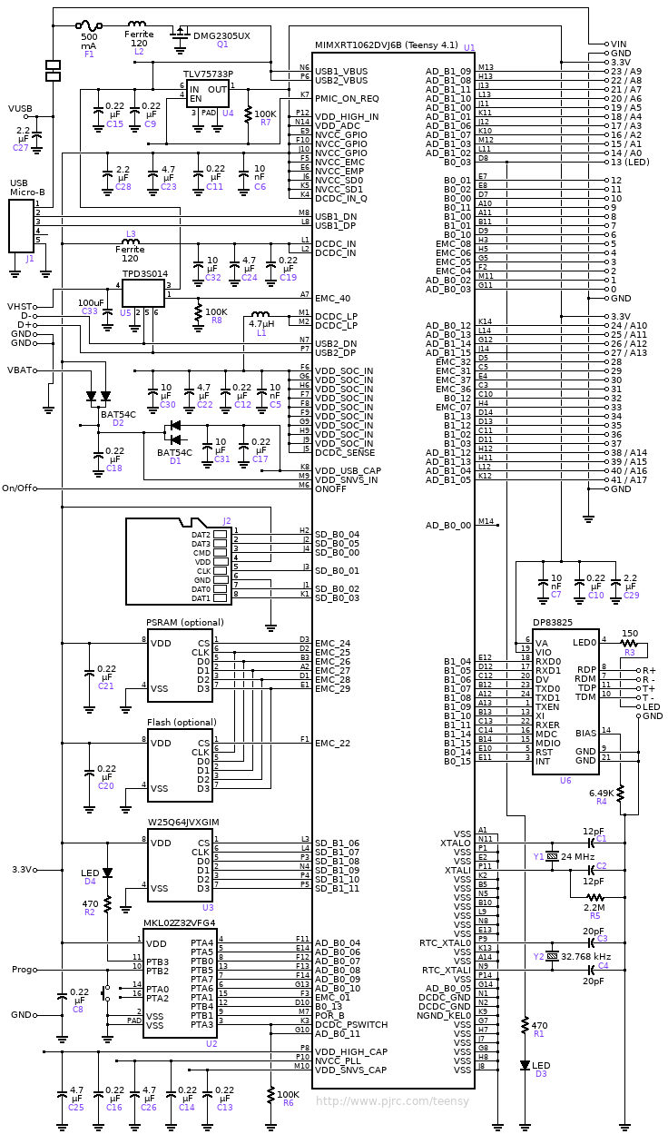
Teensy 4.1 Schematic
|
|
|
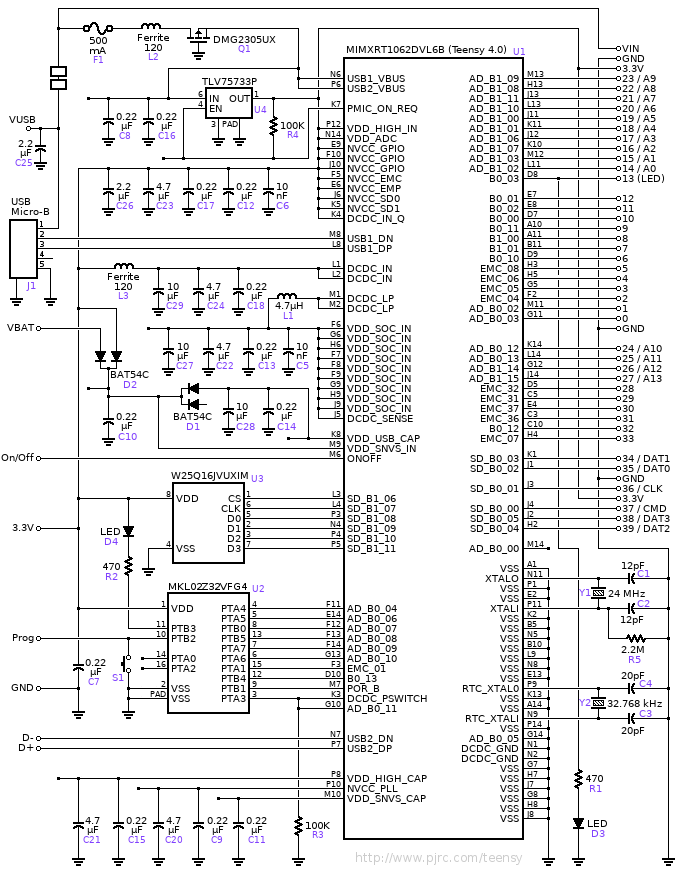
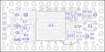
Teensy 4.0 Schematic
| |
|
|
Teensy 3.5 & 3.6 Schematic

|
|
Teensy 3.2 Schematic
|
|
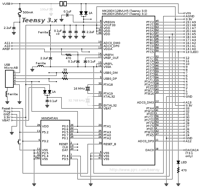
Teensy 3.0 & 3.1 Schematic
|
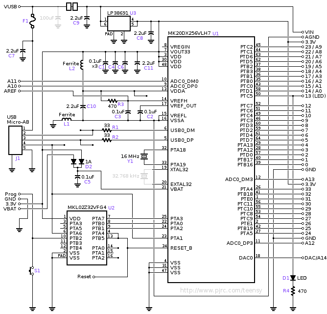
A pair of pads are linked to join VUSB to VIN. For applications where external power is needed, these pads may be cut apart to isolate the board's VIN power from VUSB.
A 32.768 kHz crystal (shown in gray) may be added to support the real time clock feature. A 100 uF capacitor (shown in gray) may be added for USB host applications, where power applied at VUSB or VIN is not capable of supplying inrush current to USB devices.
Teensy 3.1 added one signal, "DAC/A14", which was not present on Teensy 3.0. The reset signal moved from the right hand side to a test point on the bottom side. Other than this minor change, Teensy 3.0 and 3.1 are exactly the same schematic.
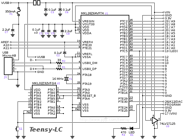
Teensy-LC Schematic
|
|
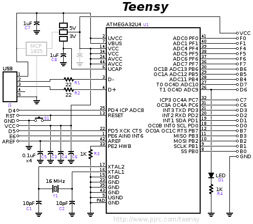
Teensy 2.0 Schematic
|
|
A 3.3 volt MCP1825 voltage regulator (shown in gray, full part number MCP1825S-3302E/DB) may be soldered to the bottom side. Three pads allow a solder bridge to configure for 5 volt or 3.3 volt power. The 5 volt pads are linked when the board is shipped.
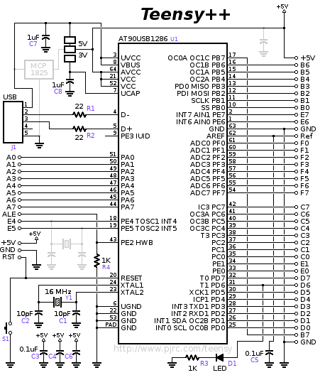
Teensy++ 2.0 Schematic
|
|
A 3.3 volt MCP1825 voltage regulator (shown in gray, full part number MCP1825S-3302E/DB) may be soldered to the bottom side. Three pads allow a solder bridge to configure for 5 volt or 3.3 volt power. The 5 volt pads are linked when the board is shipped.
Four extra parts may be soldered to the bottom side of the Teensy++. These are shown in gray. A 32768 Hz crystal may be connected to E4 & E5 for the timer2 oscillator. An extra power supply decoupling capacitor may also be added, located close to the AVcc pin.
The ALE pad should only be used as an output signal. If this pin is driven high while the reset button is pressed and released, the board will not run the Halfkay bootloader.
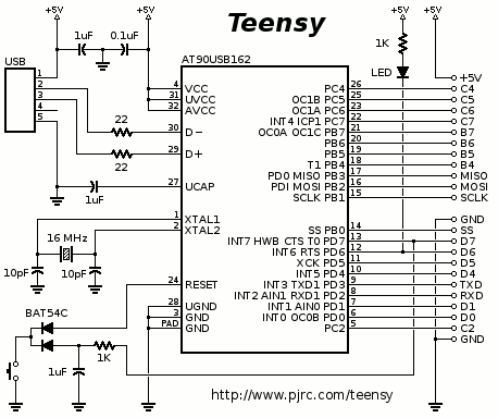
Teensy 1.0 Schematic
|
The D7 pin requires special care, because it is also the HWB signal that determines if a reset pulse will reboot to the bootloader or the user application. The simplest way to use D7 as an output, driving a load to ground (but not a pullup resistor), or as an input for a normally low or open collector type signal. If a circuit is attached to D7 that acts as a pullup resistor, it could charge the 1uF capacitor before the chip finishes reset and reboots.
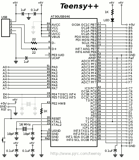
Teensy++ 1.0 Schematic
|
Four extra parts may be soldered to the bottom side of the Teensy++. These are shown in gray. A 32768 Hz crystal may be connected to E4 & E5 for the timer2 oscillator. An extra power supply decoupling capacitor may also be added, located close to the AVcc pin.