|
|
| ||
|
Shopping Cart
|
| Home | Products | Teensy | Blog | Forum |
|
You are here:
CCD Array Reader
|
|
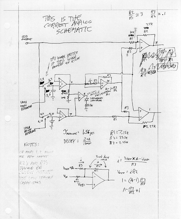
Analog Signal Processing CircuitrySomeday I'll redraw the analog schematic, but for now here's a scan of the original (ugly) hand drawn schematic that I made when I built this project.See below for explaination of how it works.
The two opamps to the left, together with the analog switches (CD4066) and 0.01 uF capacitors, are used to sample and hold the light and dark reference pixels. The control lines to those switches close the correct switch only during the appropriate pixel numbers. Refer to the LIGHT and DARK signals in the digital control schematic. If the dark reference pixel voltage is less (more light) than the light reference voltage, this indicates that the chip is exposed to so much light for long enough that it is "saturated" with stray charges. An opamp detects this condtion and turns on an LED. Not very useful, but there was an extra opamp left over. The dark reference voltage is inverted, with respect to ground, and the two rightmost opamps perform the dual function of inverting a signal and also using the negative copy of the dark reference to bring the signal so that it is referenced to ground. The opamp at the top does this for the CCD signal, and the bottom opamp does this for the light reference voltage. All of this is necessary because the TC102-1 gives signals with some unknown DC offset, where an increase in light intensity gives a lower voltage signal. How much more negative isn't known, so this analog circuitry uses the light and dark reference pixels to remove the DC offset, whatever it may happen to be at any particular time and invert the signal, so more light is indicated by a higher voltage. The automatic gain control function is achieved by feeding the upper output signal to the A/D converter's input and the lower output signal to the converter's reference input. This way, the converter's maximum code (0xFF or 255) corresponds to full illumination, regardless of the ambient light level or contrast of the image which is focused onto the array. The analog level tracking and automatic adjustment made the board able to produce high contrast output, even when a weak light source with substantial ambient background lighting was focused onto the array, as shown in the testing section. |