Bootloader Chip for DIY Teensy LC, 3.2, 3.5, 3.6 Projects
| IC_MKL02Z32_QFN16 | MKL02 chip with pre-programmed Teensy LC, 3.2, 3.5, 3.6 bootloader | $6.80 | |
| Discontinued | IC_MKL04Z32_TQFP32 | MKL04 chip with pre-programmed Teensy LC, 3.2, 3.5, 3.6 bootloader | $6.95 |
|
For developing projects, we highly recommend you use a Teensy board to get your code working.
By using this chip and a blank MKL26Z64VFT4 or MK20DX256VLH7 or MK64FX512VMD12 or MK66FX1M0VMD18, you can build your own Do-It-Yourself board that's compatible with Teensyduino and Teensy Loader. MK64FX512VLQ12 or MK66FX1M0VLQ18 (LQFP package) also work. The MKL02 or MKL04 will automatically detect which chip you've used and implement either Teensy LC, 3.2, 3.5 or 3.6.
To base your PCB design on the newer Teensy 4.x models, use this other chip.
MK20DX256VLH7, MK66FX1M0VMD18 and other parts may be out of stock at most distributors. If you're building a DIY project or just a few prototypes needing MK20DX256 or other chips, we might be able to help (of course if you're also buying this MKL02 chip). Email us to check.
MKL02/MKL04 does not implement Teensy 3.0 or 3.1. MK20DX128 is not supported.
This chip was updated on March 10, 2017 to support MK64FX512 & MK66FX1M0. Chips sold before March 10, 2017 only recognize MKL26Z64 & MK20DX256.
These chips can also be very useful for modest volume production of a fully custom product developed using Teensy LC, 3.2, 3.5 or 3.6. PJRC strongly recommends use of MKL02 for boards which may need substantial production volume. The larger MKL04 is only stocked at moderate quantity for use in prototypes and extremely low volume production.
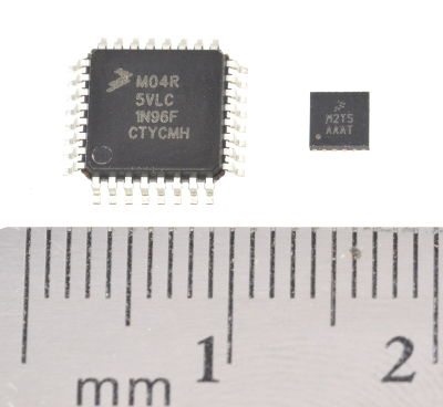
The MKL04 and MKL02 chips are functionally identical. The only difference is size. MKL02 is a tiny 3x3 mm QFN with 0.5 mm pitch pins, useful for designing the smallest possible board. MKL04 is a larger 7x7 mm TQFP part with 0.8 mm pitch pins, useful for prototyping with manual or hot plate soldering.
Required Connections:
--------------------

TQFP    QFN    Signal     Teensy 3.2            Teensy 3.5/3.6         Teensy LC
----    ---    ------     -------------         --------------         ------------
 15      7      PTA7      MK20 Pin 25 (PTA3)    MK6x Pin K7 (PTA3)     MKL26 Pin 20 (PTA3)
 16      8      PTB0      MK20 Pin 22 (PTA0)    MK6x Pin J5 (PTA0)     MKL26 Pin 17 (PTA0)
 17      9      PTB1      MK20 Pin 24 (PTA2)    MK6x Pin K6 (PTA2)
 10      6      PTA6      MK20 Pin 23 (PTA1)    MK6x Pin J6 (PTA1)
  8      4      PTA4      MK20 Pin 34 (Reset)   MK6x Pin L12 (Reset)   MKL26 Pin 26 (Reset)
 25     13      PTB5      MK20 Pin 34 (Reset)   MK6x Pin L12 (Reset)   MKL26 Pin 26 (Reset)
 18     10      PTB2                     Program Pushbutton
  7      3      PTA3                     (unused, future debug enable, see below)
  3      1      VDD                      +3.3V
  4             AVDD                     +3.3V  (TQFP only)
  5             AVSS                     Ground (TQFP only)
  6      2      VSS                      Ground
        pad     VSS                      Ground (QFN only)

All other MKL02/MKL04 pins should be left unconnected
Examples
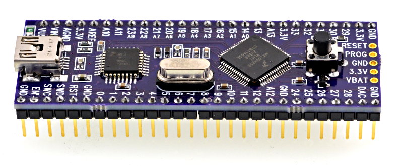
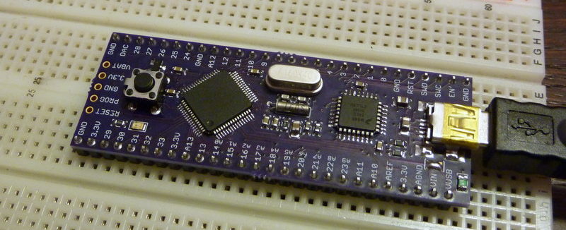
Reference Board using MKL04 chip and MK20DX256 (Teensy 3.2).
Another Reference Board designed using Eagle CAD.
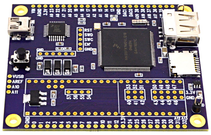
Reference Board using MKL04 chip and MK66FX1M0 (Teensy 3.6)
Crystal Guidelines
Teensy requires a 16 MHz crystal with a parallel load capacitance spec of 8 to 10 pF.If an 18 pF rated crystal is used, two 20 pF capacitors should be added to the design.
The crystal should be located close to the MK20 chip. A ground plane should be placed underneath the crystal. If using a 2 layer PCB design, the ground plane for the crystal should NOT make any other connections to ground, other than the crystal case ground, capacitor grounds (if adding extra capacitance) and to the ground pin next to the crystal pins.
Never route any digital signal directly underneath the crystal (if disregarding the ground plane advice). PCB designs that violate these rules have experienced crashes or unreliable operation due to digital signals disrupting the crystal.
Avoid routing fast digital signals in parallel with either crystal trace. Normally this is a non-issue, because ground is on one side of the crystal pins and RESET is on the other side (RESET is safe, because it's held as a DC voltage while the chip runs). Fast digital signals can capacitively couple to either crystal signal, causing the oscillator stop or jitter, which can be particularly problematic if the internal phase-locked-loop is using the crystal as its timing reference.
Poor crystal layout has caused several custom PCB designs to fail. Be careful with the crystal layout!
Future Debug Enable
Future versions will support a debug request, using the PTA3 signal. When this signal is unconnected or HIGH, the chip will function normally. When PTA3 is pulled low, future versions will tri-state all signals connected to the MK20 chip, and will ignore the Program signal.This future feature is intended to allow connecting a debug adaptor, where the cable would short PTA3 to ground. When the cable is plugged in, the MKL02/04 will effectively disconnect from all signals and allow the external debug cable full access.
Support for this debug request signal is planned for mid-2016. If you design a PCB now with a debug connector, the PTA3 signal should be connected to a pin on the debug port which the debug cable shorts to ground.
Troubleshooting
Here are conversations from people who've used the MKL02/04 or MINI54 to build their own boards. Many bits of troubleshooting advise and details are available in these forum threads!Diagnosing an unresponsive board. This discussion has details about how to check if the MK20 and MINI54 chips are alive. If you use a contract manufacturer, make sure they do not buy & use blank MINI54 chips!
Component details, particularly layout guidelines for the crystal.
VREGOUT on the MK20 must be connected, even if you are supply 3.3V without using the MK20's built in voltage regulator. The USB tranceiver power connects only to VREGOUT. Your board will fail to communicate over USB if VREGOUT does not have 3.3V power.
Good decoupling is needed on the 3.3V line. Two people confirmed their boards started working with more/better capacitors on the 3.3V power.
Pressing the pushbutton or momentarily pulling Program to GND is required on the very first use of a new board with a completely blank processor. Normally Arduino can Upload without a button press, but this only works because Teensy is running a previously-uploaded program which responds to the USB request to reboot to bootloader mode. Every brand new Teensy comes with a program properly loaded, because PJRC does a hardware test which involves pressing the button and uploading (which physically verifies the button and USB connection). When the processor is blank, or if it is running any program which doesn't properly implement USB communication, the pushbutton or a way to pull Program to logic low is required to upload your program.
Pins shorted together obviously can cause trouble. If using a contract manufacturer to assemble prototypes, make more than one board. Two or more for each comparison can help reduce chances a random construction error ruins your otherwise perfect design.
Swapping the D+ and D- signals on the USB connector causes a board with a Program and Reset signal both responding to the pushbutton (a sure sign the Mini54 works) to never actually communicate with Teensy Loader. When hard-wiring a cable, check the pinout as wire colors inside USB cables may not follow conventions.
VBAT must be connected, even if the RTC feature is never used. When VBAT lacks power, a board may be detected by Teensy Loader and appear to program correctly, but won't actually boot up and reappear as a serial device or whatever other type was selected in Tool > USB Type when compiling the code.
Missing power connections on a connector between a 2-board design can cause really confusing problems.
A strong pulldown resistor or logic low on the NMI pin can interfere with many things, incluing the bootloader's ability to program the MK20 chip. This pin has a weak pullup built into the chip, so it's safe to leave unconnected.
An accidentally deleted trace can really be frustrating. If your CAD software has an eletrical connectivity (ERC) check, use it to verify the PCB really has all nets fully connected. In Eagle, use Tools > Statistic... and search for "unroutet (airwire)".
Pin 33 PTA4 (pin 26 of the MK20 chip) must be floating or high during the first programming of the MK20 chip. This pin defaults to NMI (Non-Maskable Interrupt) when the MK20 chip is completely blank. NMI interferes with almost everything! The bootloader will disable this feature, but for the first programming of a blank MK20 chip it is enabled. PTA4 must not be pulled low until after at least 1 successful code upload.
Please understand the crystal start oscillating under software control. The oscillator is NOT automatically enabled at power-up or reset. It is perfectly normal for the crystal to not oscillate while the MK20 is held in reset state or before software activates the oscillator. The MK20 always boots up to a mode where it runs from an internal RC oscillator.
Thoughts on the business sense of making your own PCB at different volumes and points within the product lifecycle, particularly before establishing any sales trend or market demand. This technically isn't an issue with the Mini54 chip, but it's perhaps the most common "problem" with custom boards. Making your own PCB for learning or fun is always a good idea. Doing it for commercial goals can be too, but isn't necessarily always a good path.